SLASE18A September 2015 – November 2015 RF430CL331H
PRODUCTION DATA.
- 1Device Overview
- 2Revision History
- 3Terminal Configuration and Functions
-
4Specifications
- 4.1 Absolute Maximum Ratings
- 4.2 ESD Ratings
- 4.3 Recommended Operating Conditions
- 4.4 Recommended Operating Conditions, Resonant Circuit
- 4.5 Supply Currents
- 4.6 Electrical Characteristics, Digital Inputs
- 4.7 Electrical Characteristics, Digital Outputs
- 4.8 Thermal Characteristics
- 4.9 Timing and Switching Characteristics
-
5Detailed Description
- 5.1 Overview
- 5.2 Functional Block Diagram
- 5.3 Terms and Acronyms
- 5.4 Serial Communication Interface
- 5.5 Communication Protocol
- 5.6 I2C Protocol
- 5.7 NFC Type 4B Tag Platform
- 5.8 NDEF Structure
- 5.9
Typical Operation
- 5.9.1 NDEF or Capability Container Select Procedure
- 5.9.2 NDEF or Capability Container Read Binary Procedure
- 5.9.3 NDEF or Capability Container Read Procedure (Prefetch Feature)
- 5.9.4 NDEF or Capability Container Write Procedure (Blocking)
- 5.9.5 NDEF or Capability Container Write Procedure (Nonblocking)
- 5.10 RF Command Response Timing Limits
- 5.11
Registers
- 5.11.1 General Control Register
- 5.11.2 Status Register
- 5.11.3 Interrupt Registers
- 5.11.4 CRC Registers
- 5.11.5 Communication Watchdog Register
- 5.11.6 Version Register
- 5.11.7 NDEF File Identifier Register
- 5.11.8 Host Response Register
- 5.11.9 NDEF Block Length Register
- 5.11.10 NDEF File Offset Register
- 5.11.11 Buffer Start Register
- 5.11.12 SWTX Register
- 5.11.13 Custom Status Word Response Register
- 5.12 Identification
- 6Applications, Implementation, and Layout
- 7Device and Documentation Support
- 8Mechanical, Packaging, and Orderable Information
パッケージ・オプション
メカニカル・データ(パッケージ|ピン)
サーマルパッド・メカニカル・データ
- RGT|16
発注情報
6 Applications, Implementation, and Layout
NOTE
Information in the following Applications section is not part of the TI component specification, and TI does not warrant its accuracy or completeness. TI's customers are responsible for determining suitability of components for their purposes. Customers should validate and test their design implementation to confirm system functionality.
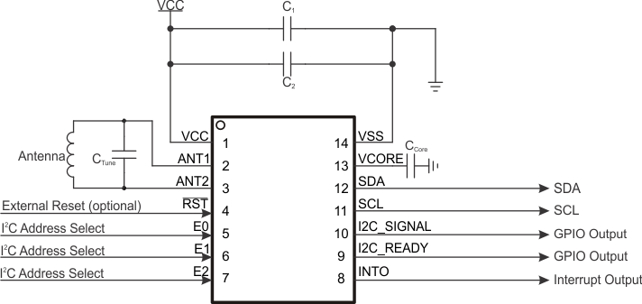
6.1 Application Diagram
Figure 6-1 shows a sample application diagram.

For recommended capacitance values, see Recommended Operating Conditions.
Figure 6-1 Application Diagram
6.2 References
- ISO/IEC 14443-2:2010, Part 2: Radio frequency interface power and signal interface (http://www.iso.org)
- ISO/IEC 14443-3:2011, Part 3: Initialization and anticollision (http://www.iso.org)
- ISO/IEC 14443-4:2008, Part 4: Transmission protocols (http://www.iso.org)
- NFC Data Exchange Format (NDEF) Technical Specification (http://nfc-forum.org/)
- NFC Forum Type 4 Tag Operation Specification (http://nfc-forum.org/)
- NFC Digital Protocol Technical Specification, Section 13.2.2, Frame Wait Time Extension (http://nfc-forum.org/)