JAJSL60F April   1977  – January 2021 SG2524 , SG3524

PRODUCTION DATA  

  1. 特長
  2. アプリケーション
  3. 概要
  4. Revision History
  5. Pin Configurations and Functions
    1.     Pin Functions
  6. Specifications
    1. 6.1 Absolute Maximum Ratings
    2. 6.2 ESD Ratings
    3. 6.3 Recommended Operating Conditions
    4. 6.4 Thermal Information
  7. 12
    1. 7.1 Electrical Characteristics
    2. 7.2 Electrical Characteristics — Continued, Both Parts
    3. 7.3 Typical Characteristics
  8. Parameter Measurement Information
    1. 8.1 17
  9. Detailed Description
    1. 9.1 Overview
    2. 9.2 Functional Block Diagram
    3. 9.3 Feature Description
      1. 9.3.1 Blanking
      2. 9.3.2 Error Amplifier
      3. 9.3.3 Compensation
      4. 9.3.4 Output Circuitry
      5. 9.3.5 Current Limiting
    4. 9.4 Device Functional Modes
      1. 9.4.1 Synchronous Operation
      2. 9.4.2 Shutdown Circuitry
        1.       Application and Implementation
          1. 10.1 Application Information
          2. 10.2 Typical Application
            1. 10.2.1 Capacitor-Diode Output
              1. 10.2.1.1 Design Requirements
              2. 10.2.1.2 Detailed Design Procedure
                1. 10.2.1.2.1 Oscillator
                2. 10.2.1.2.2 Voltage Reference
              3. 10.2.1.3 Application Curves
          3. 10.3 Examples of Other Output Stages
            1. 10.3.1 Flyback Converter
            2. 10.3.2 Single-Ended LC
            3. 10.3.3 Push-Pull Transformer-Coupled
              1.          Power Supply Recommendations
  10. 10Layout
    1. 10.1 Layout Guidelines
      1. 10.1.1 Feedback Traces
      2. 10.1.2 Input/Output Capacitors
      3. 10.1.3 Compensation Components
      4. 10.1.4 Traces and Ground Planes
    2. 10.2 Layout Example
  11. 11Device and Documentation Support
    1. 11.1 Related Links
    2. 11.2 Trademarks
      1.      Mechanical, Packaging, and Orderable Information

パッケージ・オプション

デバイスごとのパッケージ図は、PDF版データシートをご参照ください。

メカニカル・データ(パッケージ|ピン)
  • NS|16
  • N|16
  • D|16
サーマルパッド・メカニカル・データ
発注情報

Current Limiting

A current-limiting sense amplifier is provided in the SGx524 device. The current-limiting sense amplifier exhibits a threshold of 200 mV ±25 mV and must be applied in the ground line since the voltage range of the inputs is limited to 1 V to –1 V. Caution should be taken to ensure the –1-V limit is not exceeded by either input, otherwise, damage to the device may result.

Foldback current limiting can be provided with the network shown in Figure 9-1. The current-limit schematic is shown in Figure 9-2.

GUID-4EA73246-0E89-4907-A9D9-34076DC4E3B3-low.gifFigure 9-1 Foldback Current Limiting for Shorted Output Conditions
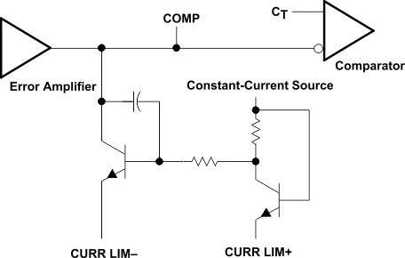
GUID-317BA511-6986-4617-93BC-91675EBCE7B5-low.gifFigure 9-2 Current-Limit Schematic