JAJSUE5A April   2024  – July 2024 SN4599-Q1

PRODUCTION DATA  

  1.   1
  2. 特長
  3. アプリケーション
  4. 概要
  5. Pin Configuration and Functions
  6. Specifications
    1. 5.1 Absolute Maximum Ratings
    2. 5.2 ESD Ratings
    3. 5.3 Recommended Operating Conditions
    4. 5.4 Thermal Information
    5. 5.5 Source or Drain Current through Switch
    6. 5.6 Electrical Characteristics
    7. 5.7 Analog Channel Specifications
    8. 5.8 Switching Characteristics
    9. 5.9 Typical Characteristics
  7. Parameter Measurement Information
    1. 6.1 On-Resistance
    2. 6.2 Off-Leakage Current
    3. 6.3 On-Leakage Current
    4. 6.4 Transition Time
    5. 6.5 Break-Before-Make
    6. 6.6 Charge Injection
    7. 6.7 Off Isolation
    8. 6.8 Crosstalk
    9. 6.9 Bandwidth
  8. Detailed Description
    1. 7.1 Functional Block Diagram
    2. 7.2 Feature Description
      1. 7.2.1 Bidirectional Operation
      2. 7.2.2 Rail to Rail Operation
      3. 7.2.3 Fail-Safe Logic
    3. 7.3 Device Functional Modes
    4. 7.4 Truth Tables
  9. Application and Implementation
    1. 8.1 Application Information
    2. 8.2 Typical Application
      1. 8.2.1 Switchable Operational Amplifier Gain Setting
        1. 8.2.1.1 Design Requirements
        2. 8.2.1.2 Detailed Design Procedure
        3. 8.2.1.3 Application Curve
      2. 8.2.2 Input Control for Power Amplifier
        1. 8.2.2.1 Design Requirements
        2. 8.2.2.2 Detailed Design Procedure
        3. 8.2.2.3 Application Curve
    3. 8.3 Power Supply Recommendations
    4. 8.4 Layout
      1. 8.4.1 Layout Guidelines
      2. 8.4.2 Layout Example
  10. Device and Documentation Support
    1. 9.1 Documentation Support
      1. 9.1.1 Related Documentation
    2. 9.2 ドキュメントの更新通知を受け取る方法
    3. 9.3 サポート・リソース
    4. 9.4 Trademarks
    5. 9.5 静電気放電に関する注意事項
    6. 9.6 用語集
  11. 10Revision History
  12. 11Mechanical, Packaging, and Orderable Information
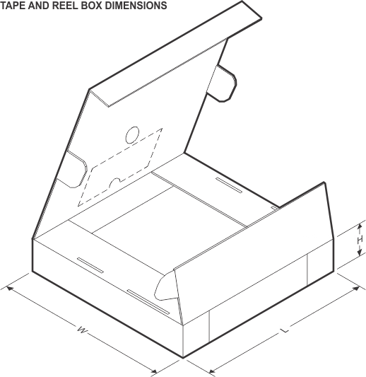
    1. 11.1 Tape and Reel Information
    2. 11.2 Mechanical Data

パッケージ・オプション

デバイスごとのパッケージ図は、PDF版データシートをご参照ください。

メカニカル・データ(パッケージ|ピン)
  • DBV|6
サーマルパッド・メカニカル・データ
発注情報

Tape and Reel Information

SN4599-Q1
Device Package
Type
Package Drawing Pins SPQ Reel
Diameter (mm)
Reel
Width W1 (mm)
A0
(mm)
B0
(mm)
K0
(mm)
P1
(mm)
W
(mm)
Pin1
Quadrant
SN4599DBVRQ1 SOT-23 DBV 6 3000 178 9 2.4 2.5 1.2 4 8 Q3
SN4599-Q1
Device Package Type Package Drawing Pins SPQ Length (mm) Width (mm) Height (mm)
SN4599DBVRQ1 SOT-23 DBV 6 3000 180 180 18