JAJSGI2I september   2015  – august 2023 SN6505A , SN6505B

PRODUCTION DATA  

  1.   1
  2. 特長
  3. アプリケーション
  4. 概要
  5. Revision History
  6. Pin Configuration and Functions
  7. Specifications
    1. 6.1 Absolute Maximum Ratings
    2. 6.2 ESD Ratings
    3. 6.3 Recommended Operating Conditions
    4. 6.4 Thermal Information
    5. 6.5 Electrical Characteristics
    6. 6.6 Timing Requirements
    7. 6.7 Typical Characteristics, SN6505A
    8. 6.8 Typical Characteristics, SN6505B
  8. Parameter Measurement Information
  9. Detailed Description
    1. 8.1 Overview
    2. 8.2 Functional Block Diagram
    3. 8.3 Feature Description
      1. 8.3.1 Push-Pull Converter
      2. 8.3.2 Core Magnetization
    4. 8.4 Device Functional Modes
      1. 8.4.1 Start-Up Mode
        1. 8.4.1.1 Soft-Start
      2. 8.4.2 Operating Mode
      3. 8.4.3 Shutdown-Mode
      4. 8.4.4 Spread Spectrum Clocking
      5. 8.4.5 External Clock Mode
  10. Application and Implementation
    1. 9.1 Application Information
    2. 9.2 Typical Application
      1. 9.2.1 Design Requirements
      2. 9.2.2 Detailed Design Procedure
        1. 9.2.2.1 Drive Capability
        2. 9.2.2.2 LDO Selection
        3. 9.2.2.3 Diode Selection
        4. 9.2.2.4 Capacitor Selection
        5. 9.2.2.5 Transformer Selection
          1. 9.2.2.5.1 V-t Product Calculation
          2. 9.2.2.5.2 Turns Ratio Estimate
          3. 9.2.2.5.3 Recommended Transformers
      3. 9.2.3 Application Curves
      4. 9.2.4 System Examples
        1. 9.2.4.1 Higher Output Voltage Designs
        2. 9.2.4.2 Application Circuits
  11. 10Power Supply Recommendations
  12. 11Layout
    1. 11.1 Layout Guidelines
    2. 11.2 Layout Example
  13. 12Device and Documentation Support
    1. 12.1 Device Support
    2. 12.2 Documentation Support
      1. 12.2.1 Related Documentation
    3. 12.3 Related Links
    4. 12.4 Receiving Notification of Documentation Updates
    5. 12.5 Community Resources
    6. 12.6 Trademarks
  14. 13Mechanical, Packaging, and Orderable Information

パッケージ・オプション

メカニカル・データ(パッケージ|ピン)
サーマルパッド・メカニカル・データ
発注情報

Diode Selection

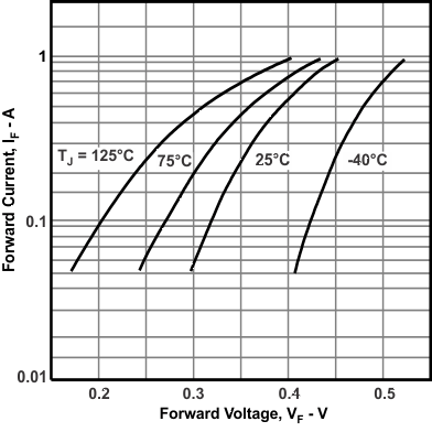
A rectifier diode should always possess low-forward voltage to provide as much voltage to the converter output as possible. When used in high-frequency switching applications, such as the SN6505 however, the diode must also possess a short recovery time. Schottky diodes meet both requirements and are therefore strongly recommended in push-pull converter designs. A good choice for low-volt applications and ambient temperatures of up to 85°C is the low-cost Schottky rectifier MBR0520L with a typical forward voltage of 275 mV at 100-mA forward current. For higher output voltages such as ±10 V and above use the MBR0530 which provides a higher DC blocking voltage of 30 V.

Lab measurements have shown that at temperatures higher than 100°C the leakage currents of the above Schottky diodes increase significantly. This can cause thermal runaway leading to the collapse of the rectifier output voltage. Therefore, for ambient temperatures higher than 85°C use low-leakage Schottky diodes, such as RB168MM-40.
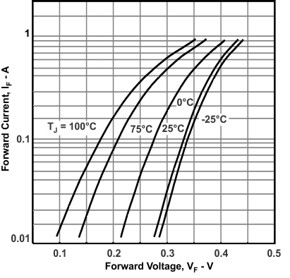
GUID-5AAFB168-D454-4C3E-AC5E-88ED75DF05D8-low.gifFigure 9-4 Diode Forward Characteristics for MBR0520L
GUID-6202280C-BBE7-405C-8906-16F1CACA3D57-low.gifFigure 9-5 Diode Forward Characteristics MBR0530