JAJSGI2I september 2015 – august 2023 SN6505A , SN6505B
PRODUCTION DATA
- 1
- 1 特長
- 2 アプリケーション
- 3 概要
- 4 Revision History
- 5 Pin Configuration and Functions
- 6 Specifications
- 7 Parameter Measurement Information
- 8 Detailed Description
- 9 Application and Implementation
- 10Power Supply Recommendations
- 11Layout
- 12Device and Documentation Support
- 13Mechanical, Packaging, and Orderable Information
9.2.2.5.2 Turns Ratio Estimate
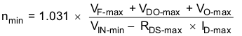
Assume the rectifier diodes and linear regulator has been selected. Also, it has been determined that the transformer chosen must have a V-t product of at least 11 Vμs. However, before searching the manufacturer web sites for a suitable transformer, the user still needs to know its minimum turns ratio that allows the push-pull converter to operate flawlessly over the specified current and temperature range. This minimum transformation ratio is expressed through the ratio of minimum secondary to minimum primary voltage multiplied by a correction factor that takes the transformer’s typical efficiency of 97% into account:
VS-min must be large enough to allow for a maximum voltage drop, VF-max, across the rectifier diode and still provide sufficient input voltage for the regulator to remain in regulation. From the Section 9.2.2.2 section, this minimum input voltage is known and by adding VF-max gives the minimum secondary voltage with:
 Figure 9-6 Establishing the Required Minimum Turns Ratio Through Nmin = 1.031 × VS-min / VP-min
Then calculating the available minimum primary voltage, VP-min, involves subtracting the maximum possible drain-source voltage of the device, VDS-max, from the minimum converter input voltage VIN-min:
VDS-max however, is the product of the maximum RDS(on) and ID values for a given supply specified in the data sheet:
Then inserting Equation 8 into Equation 7 yields:
and inserting Equation 9 and Equation 6 into Equation 5 provides the minimum turns ration with:
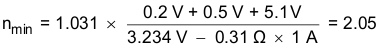
Example:
For a 3.3 VIN to 5 VOUT converter using the rectifier diode MBR0520L and the 5 V LDO, the data sheet values taken for a load current of 600 mA and a maximum temperature of 85°C are VF-max = 0.2 V,
VDO-max = 0.5 V, and VO-max = 5.1 V.
Then assuming that the converter input voltage is taken from a 3.3 V controller supply with a maximum ±2% accuracy makes VIN-min = 3.234 V. Finally the maximum values for drain-source resistance and drain current at 3.3 V are taken from the data sheet with RDS-max = 0.31 Ω and ID-max = 1 A.
Inserting the values above into Equation 10 yields a minimum turns ratio of:
Most commercially available transformers for 3-to-5 V push-pull converters offer turns ratios between 2.0 and 2.3 with a common tolerance of ±3%.