JAJSPU9M september 2005 – february 2023 SN65HVD30 , SN65HVD31 , SN65HVD32 , SN65HVD33 , SN65HVD34 , SN65HVD35
PRODUCTION DATA
- 1 特長
- 2 アプリケーション
- 3 概要
- 4 Revision History
- 5 Device Comparison
- 6 Pin Configuration and Functions
-
7 Specifications
- 7.1 Absolute Maximum Ratings
- 7.2 ESD Ratings
- 7.3 Recommended Operating Conditions
- 7.4 Thermal Information
- 7.5 Electrical Characteristics: Driver
- 7.6 Electrical Characteristics: Receiver
- 7.7 Device Power Dissipation – PD
- 7.8 Supply Current Characteristics
- 7.9 Switching Characteristics: Driver
- 7.10 Switching Characteristics: Receiver
- 7.11 Dissipation Ratings
- 7.12 Typical Characteristics
- 8 Detailed Description
- 9 Application and Implementation
- 10Device and Documentation Support
- 11Mechanical, Packaging, and Orderable Information
パッケージ・オプション
メカニカル・データ(パッケージ|ピン)
- D|14
サーマルパッド・メカニカル・データ
- D|14
発注情報
8.3.5 Safe Operation With Bus Contention
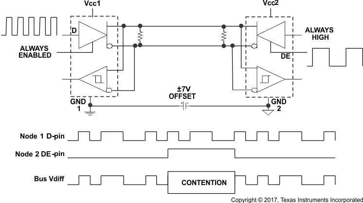
These devices incorporate a driver current limit of 250 mA across the RS-485 common-mode range of –7 V to +12 V. As stated in the Application Guidelines for TIA/EIA-485-A(1), this sets a practical limitation to prevent damage during bus contention events. Contention can occur during system initialization, during system faults, or whenever two or more drivers are active at the same time.
Figure 8-3 shows a 2-node system to demonstrate bus contention by forcing both drivers to be active in opposing states.
 Figure 8-3 Bus Contention Example
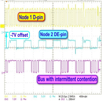
Figure 8-4 shows typical operation in a bus contention event. The bottom trace illustrates how the SN65HVD33 device at Node 1 continues normal operation after a contention event between the two drivers with a –7-V ground offset on Node 2. This illustrates how the SN65HVD3x family of devices operates robustly in spite of bus contention faults, even with large common-mode offsets.
 Figure 8-4 SN65HVD3x Drivers Operate Correctly After Bus Contention Faults