JAJSPU9M september 2005 – february 2023 SN65HVD30 , SN65HVD31 , SN65HVD32 , SN65HVD33 , SN65HVD34 , SN65HVD35
PRODUCTION DATA
- 1 特長
- 2 アプリケーション
- 3 概要
- 4 Revision History
- 5 Device Comparison
- 6 Pin Configuration and Functions
-
7 Specifications
- 7.1 Absolute Maximum Ratings
- 7.2 ESD Ratings
- 7.3 Recommended Operating Conditions
- 7.4 Thermal Information
- 7.5 Electrical Characteristics: Driver
- 7.6 Electrical Characteristics: Receiver
- 7.7 Device Power Dissipation – PD
- 7.8 Supply Current Characteristics
- 7.9 Switching Characteristics: Driver
- 7.10 Switching Characteristics: Receiver
- 7.11 Dissipation Ratings
- 7.12 Typical Characteristics
- 8 Detailed Description
- 9 Application and Implementation
- 10Device and Documentation Support
- 11Mechanical, Packaging, and Orderable Information
パッケージ・オプション
メカニカル・データ(パッケージ|ピン)
- D|14
サーマルパッド・メカニカル・データ
- D|14
発注情報
6 Pin Configuration and Functions
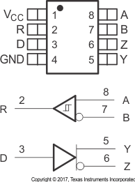
 Figure 6-1 SN65HVD30, SN65HVD31, SN65HVD32, D Package8-Pin SOICTop View
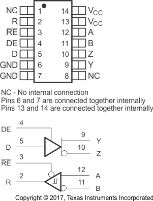
 Figure 6-2 SN65HVD33, SN65HVD34, SN65HVD35 D Package14-Pin SOICTop View
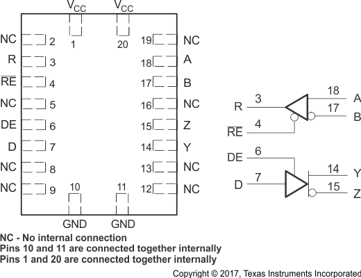
 Figure 6-3 SN65HVD33 RHL Package 20-Pin VQFNTop View
Table 6-1 Pin Functions
| PIN | TYPE | DESCRIPTION | |||
|---|---|---|---|---|---|
| NAME | D (8-Pins) |
D (14-Pins) |
RHL (20-Pins) |
||
| A | 8 | 12 | 18 | Bus input | Receiver input (complementary to B) |
| B | 7 | 11 | 17 | Bus input | Receiver input (complementary to A) |
| D | 3 | 5 | 7 | Digital input | Driver data input |
| DE | — | 4 | 6 | Digital input | Driver enable, active high |
| GND | 4 | 6, 7 | 10, 11 | Reference potential | Local device ground |
| NC | — | 1, 8 | 2, 5, 8, 9, 12, 13, 16, 19 |
No connect | No connect; must be left floating |
| R | 2 | 2 | 3 | Digital output | Receive data output |
| RE | — | 3 | 4 | Digital output | Receiver enable, active low |
| VCC | 1 | 13, 14 | 1, 20 | Supply | 3-V to 3.6-V supply |
| Y | 5 | 9 | 14 | Bus output | Driver output (complementary to Z) |
| Z | 6 | 10 | 15 | Bus output | Driver output (complementary to Y) |