JAJSGU3H March 2012 – March 2019 SN65HVD72 , SN65HVD75 , SN65HVD78
UNLESS OTHERWISE NOTED, this document contains PRODUCTION DATA.
- 1 特長
- 2 アプリケーション
- 3 概要
- 4 改訂履歴
- 5 Device Comparison Table
- 6 Pin Configuration and Functions
-
7 Specifications
- 7.1 Absolute Maximum Ratings
- 7.2 ESD Ratings
- 7.3 Recommended Operating Conditions
- 7.4 Thermal Information
- 7.5 Electrical Characteristics
- 7.6 Power Dissipation
- 7.7 Switching Characteristics: 250 kbps Device (SN65HVD72) Bit Time ≥ 4 µs
- 7.8 Switching Characteristics: 20 Mbps Device (SN65HVD75) Bit Time ≥50 ns
- 7.9 Switching Characteristics: 50 Mbps Device (SN65HVD78) Bit Time ≥20 ns
- 7.10 Typical Characteristics
- 8 Parameter Measurement Information
- 9 Detailed Description
- 10Application and Implementation
- 11Power Supply Recommendations
- 12Layout
- 13デバイスおよびドキュメントのサポート
- 14メカニカル、パッケージ、および注文情報
パッケージ・オプション
メカニカル・データ(パッケージ|ピン)
サーマルパッド・メカニカル・データ
- DRB|8
発注情報
10.2.2.2 Isolated Bus Node Design
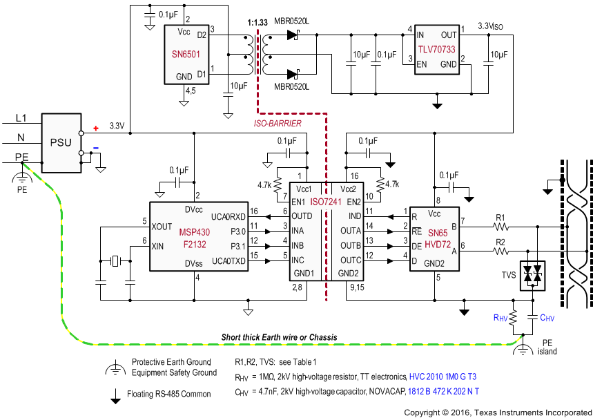
Many RS-485 networks use isolated bus nodes to prevent the creation of unintended ground loops and their disruptive impact on signal integrity. An isolated bus node typically includes a microcontroller that connects to the bus transceiver via a multi-channel, digital isolator (Figure 27).
 Figure 27. Isolated Bus Node with Transient Protection
 Power isolation is accomplished using the push-pull transformer driver SN6501 and a low-cost LDO, TLV70733.
Signal isolation uses the quadruple digital isolator ISO7241. Notice that both enable inputs, EN1 and EN2, are pulled up via 4.7 kΩ resistors to limit their input currents during transient events.
While the transient protection is similar to the one in Figure 26 (left circuit), an additional high-voltage capacitor is used to divert transient energy from the floating RS-485 common further towards Protective Earth (PE) ground. This is necessary as noise transients on the bus are usually referred to Earth potential.
RHV refers to a high voltage resistor, and in some applications even a varistor. This resistance is applied to prevent charging of the floating ground to dangerous potentials during normal operation.
Occasionally varistors are used instead of resistors to rapidly discharge CHV, if it is expected that fast transients might charge CHV to high-potentials.
Note that the PE island represents a copper island on the PCB for the provision of a short, thick Earth wire connecting this island to PE ground at the entrance of the power supply unit (PSU).
In equipment designs using a chassis, the PE connection is usually provided through the chassis itself. Typically the PE conductor is tied to the chassis at one end while the high-voltage components, CHV and RHV, are connecting to the chassis at the other end.