JAJSPH1E May 2000 – January 2023 SN65LBC179A , SN75LBC179A
PRODUCTION DATA
- 1特長
- 2概要
- 3Revision History
- 4Pin Configuration and Functions
- 5Specifications
- 6Parameter Measurement Information
- 7Detailed Description
- 8Device and Documentation Support
- 9Mechanical, Packaging, and Orderable Information
パッケージ・オプション
メカニカル・データ(パッケージ|ピン)
サーマルパッド・メカニカル・データ
発注情報
4 Pin Configuration and Functions
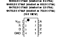
Table 4-1 Pin Functions
| NO | Name | Type | Description |
|---|---|---|---|
| 1 | VCC | Supply | 4.75V to 5.25V Supply |
| 2 | R | O | Receive data output |
| 3 | D | I | Driver data input |
| 4 | GND | GND | Device ground |
| 5 | Y | O | Digital bus output, Y (Complementary to Z) |
| 6 | Z | O | Digital bus output, Z (Complementary to Y) |
| 7 | B | I | Bus input, B (complementary to A) |
| 8 | A | I | Bus input, A (complementary to B) |