JAJSPH1E May 2000 – January 2023 SN65LBC179A , SN75LBC179A
PRODUCTION DATA
- 1特長
- 2概要
- 3Revision History
- 4Pin Configuration and Functions
- 5Specifications
- 6Parameter Measurement Information
- 7Detailed Description
- 8Device and Documentation Support
- 9Mechanical, Packaging, and Orderable Information
パッケージ・オプション
メカニカル・データ(パッケージ|ピン)
サーマルパッド・メカニカル・データ
発注情報
6 Parameter Measurement Information
 Figure 6-1 Driver VOD and VOC
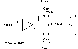
 Figure 6-2 Driver VOD With Common-Mode Loading
A. The input pulse is supplied by a generator having the following characteristics: PRR ≤ 1 MHz, 50% duty cycle, tr ≤ 6 ns, tf ≤ 6 ns, ZO = 50 Ω.
B. CL includes probe and jig capacitance.
Figure 6-3 Driver Test Circuits and Voltage Waveforms
A. The input pulse is supplied by a generator having the following characteristics: PRR ≤ 1 MHz, 50% duty cycle, tr ≤ 6 ns, tf ≤ 6 ns, ZO = 50 Ω.
B. CL includes probe and jig capacitance.
Figure 6-4 Receiver Test Circuit and Voltage Waveforms