JAJSF06A March 2018 – May 2018 SN65LVDS93B
PRODUCTION DATA.
7.7 Switching Characteristics
over operating free-air temperature range (unless otherwise noted)| TEST CONDITIONS | MIN | TYP(1) | MAX | UNIT | ||
|---|---|---|---|---|---|---|
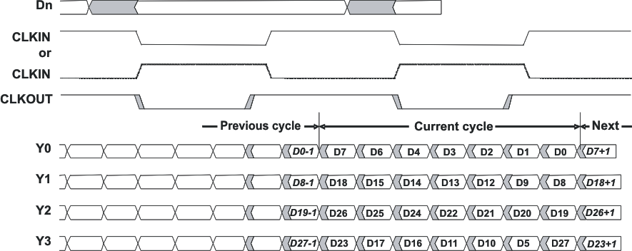
| t0 | Delay time, CLKOUT↑ after Yn valid (serial bit position 0, equal D1, D9, D20, D5) | See Figure 8, tC = 10 ns,
|Input clock jitter| < 25 ps (2) |
–0.1 | 0 | 0.1 | ns |
| t1 | Delay time, CLKOUT↑ after Yn valid (serial bit position 1, equal D0, D8, D19, D27) | 1/7 tc – 0.1 | 1/7 tc + 0.1 | ns | ||
| t2 | Delay time, CLKOUT↑ after Yn valid (serial bit position 2, equal D7, D18, D26. D23) | 2/7 tc – 0.1 | 2/7 tc + 0.1 | ns | ||
| t3 | Delay time, CLKOUT↑ after Yn valid (serial bit position 3; equal D6, D15, D25, D17) | 3/7 tc – 0.1 | 3/7 tc + 0.1 | ns | ||
| t4 | Delay time, CLKOUT↑ after Yn valid (serial bit position 4, equal D4, D14, D24, D16) | 4/7 tc – 0.1 | 4/7 tc + 0.1 | ns | ||
| t5 | Delay time, CLKOUT↑ after Yn valid (serial bit position 5, equal D3, D13, D22, D11) | 5/7 tc – 0.1 | 5/7 tc + 0.1 | ns | ||
| t6 | Delay time, CLKOUT↑ after Yn valid (serial bit position 6, equal D2, D12, D21, D10) | 6/7 tc – 0.1 | 6/7 tc + 0.1 | ns | ||
| tc(o) | Output clock period | tc | ns | |||
| Δtc(o) | Output clock cycle-to-cycle jitter (3) | tC = 10 ns; clean reference clock, see Figure 9 | ±35 | ps | ||
| tC = 10 ns with 0.05UI added noise modulated at 3 MHz, see Figure 9 | ±44 | |||||
| tC = 7.4 ns; clean reference clock, see Figure 9 | ±35 | |||||
| tC = 7.4 ns with 0.05UI added noise modulated at 3 MHz, see Figure 9 | ±42 | |||||
| tw | High-level output clock pulse duration | 4/7 tc | ns | |||
| tr/f | Differential output voltage transition time (tr or tf) | See Figure 5 | 225 | 500 | ps | |
| ten | Enable time, SHTDN↑ to phase lock (Yn valid) | f(clk) = 85 MHz, See Figure 10 | 10 | µs | ||
| tdis | Disable time, SHTDN↓ to off-state (CLKOUT high-impedance) | f(clk) = 85 MHz, See Figure 11 | 12 | ns | ||
(1) All typical values are at VCC = 3.3V,TA = 25°C.
(2) |Input clock jitter| is the magnitude of the change in theinputclock period.
(3) The output clock cycle-to-cycle jitter is the largestrecordedchange in the output clock period from one cycle to the next cycle observed over15,000cycles.Tektronix TDSJIT3 Jitter Analysis software was used to derive the maximum and minimumjittervalue.
 Figure 1. Typical SN65LVDS93B Load and Shift Sequences