JAJSKL9B September 2020 – November 2022 SN65MLVD203B
PRODUCTION DATA
- 1 特長
- 2 アプリケーション
- 3 概要
- 4 Revision History
- 5 Pin Configuration and Functions
- 6 Specifications
- 7 Parameter Measurement Information
- 8 Detailed Description
-
9 Application and Implementation
- 9.1 Application Information
- 9.2
Typical Application
- 9.2.1 Multipoint Communications
- 9.2.2 Design Requirements
- 9.2.3
Detailed Design Procedure
- 9.2.3.1 Supply Voltage
- 9.2.3.2 Supply Bypass Capacitance
- 9.2.3.3 Driver Input Voltage
- 9.2.3.4 Driver Output Voltage
- 9.2.3.5 Termination Resistors
- 9.2.3.6 Receiver Input Signal
- 9.2.3.7 Receiver Input Threshold (Failsafe)
- 9.2.3.8 Receiver Output Signal
- 9.2.3.9 Interconnecting Media
- 9.2.3.10 PCB Transmission Lines
- 9.2.4 Application Curves
- 9.3 Power Supply Recommendations
- 9.4 Layout
- 10Device and Documentation Support
- 11Mechanical, Packaging, and Orderable Information
パッケージ・オプション
メカニカル・データ(パッケージ|ピン)
- RUM|16
サーマルパッド・メカニカル・データ
- RUM|16
発注情報
9.4.1.1 Microstrip vs. Stripline Topologies
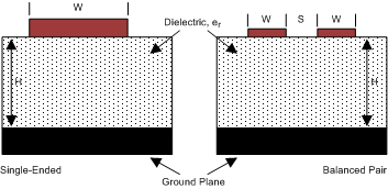
As per SLLD009, printed-circuit boards usually offer designers two transmission line options: Microstrip and stripline. Microstrips are traces on the outer layer of a PCB, as shown in Figure 9-7.
 Figure 9-7 Microstrip Topology
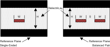
On the other hand, striplines are traces between two ground planes. Striplines are less prone to emissions and susceptibility problems because the reference planes effectively shield the embedded traces. However, from the standpoint of high-speed transmission, juxtaposing two planes creates additional capacitance. TI recommends routing M-LVDS signals on microstrip transmission lines if possible. The PCB traces allow designers to specify the necessary tolerances for ZO based on the overall noise budget and reflection allowances. Footnotes 11, 22, and 33 provide formulas for ZO and tPD for differential and single-ended traces. (2)(3)(4)
 Figure 9-8 Stripline Topology