SCES644D MARCH 2006 – December 2015 SN74AUP1G74
PRODUCTION DATA.
- 1 Features
- 2 Applications
- 3 Description
- 4 Revision History
- 5 Pin Configuration and Functions
-
6 Specifications
- 6.1 Absolute Maximum Ratings
- 6.2 ESD Ratings
- 6.3 Recommended Operating Conditions
- 6.4 Thermal Information
- 6.5 Electrical Characteristics, TA = 25°C
- 6.6 Electrical Characteristics, TA = -40°C to +85°C
- 6.7 Timing Requirements
- 6.8 Switching Characteristics, CL = 5 pF
- 6.9 Switching Characteristics, CL = 10 pF
- 6.10 Switching Characteristics, CL = 15 pF
- 6.11 Switching Characteristics, CL = 30 pF
- 6.12 Operating Characteristics
- 6.13 Typical Characteristics
- 7 Parameter Measurement Information
- 8 Detailed Description
- 9 Application and Implementation
- 10Power Supply Recommendations
- 11Layout
- 12Device and Documentation Support
- 13Mechanical, Packaging, and Orderable Information
パッケージ・オプション
メカニカル・データ(パッケージ|ピン)
サーマルパッド・メカニカル・データ
発注情報
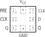
5 Pin Configuration and Functions
DCU Package
8-Pin VSSOP
Top View

RSE Package
8-Pin UQFN
Top View

DQE Package
8-Pin X2SON
Top View

YFP or YZP Package
8-Pin DSBGA
Top View

Pin Functions(1)
| PIN | I/O | DESCRIPTION | |||
|---|---|---|---|---|---|
| NAME | VSSOP, X2SON | UQFN | DSBGA | ||
| CLK | 1 | 7 | A1 | I | Rising edge triggered clock signal input |
| CLR | 6 | 2 | C2 | I | Clear, Active low |
| D | 2 | 6 | B1 | I | Data input |
| GND | 4 | 4 | D1 | — | Ground |
| PRE | 7 | 1 | B2 | I | Preset, Active low |
| Q | 5 | 3 | D2 | O | Output |
| Q | 3 | 5 | C1 | O | Inverted output |
| VCC | 8 | 8 | A2 | — | Power supply |
(1) See Mechanical, Packaging, and Orderable Information for dimensions.