JAJSJI0D September 1988 – February 2021 SN74BCT374
PRODUCTION DATA
- 1 特長
- 2 アプリケーション
- 3 概要
- 4 Revision History
- 5 Pin Configuration and Functions
- 6 Specifications
- 7 Parameter Measurement Information
- 8 Detailed Description
- 9 Application and Implementation
- 10Power Supply Recommendations
- 11Layout
- 12Device and Documentation Support
- 13Mechanical, Packaging, and Orderable Information
パッケージ・オプション
デバイスごとのパッケージ図は、PDF版データシートをご参照ください。
メカニカル・データ(パッケージ|ピン)
- NS|20
- N|20
- DW|20
サーマルパッド・メカニカル・データ
発注情報
7 Parameter Measurement Information
All parameters and waveforms are not applicable to all devices.
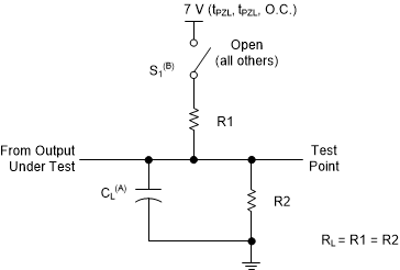
A. CL includes probe and jig capacitance.
B. When measuring propagation delay times of 3-state outputs, switch S1 is
open.
Figure 7-1 Load circuit for3-state and open-collector outputs
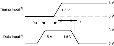
A. All input pulses are supplied by generators having the following
characteristics: PRR ≤ 10 MHz, tr = tf ≤ 2.5 ns, duty
cycle = 50%.
Figure 7-3 Voltage waveformsSetup and hold times
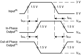
A. The outputs are measured one at a time with one transition per
measurement.
B. All input pulses are supplied by generators having the following
characteristics: PRR ≤ 10 MHz, tr = tf ≤ 2.5 ns, duty
cycle = 50%.
Figure 7-5 Voltage waveformsPropagation delay times
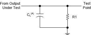
A. CL includes probe and jig capacitance.
Figure 7-2 Load circuit forpush-pull outputs
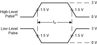
A. All input pulses are supplied by generators having the following
characteristics: PRR ≤ 10 MHz, tr = tf ≤ 2.5 ns, duty
cycle = 50%.
Figure 7-4 Voltage waveformsPulse duration
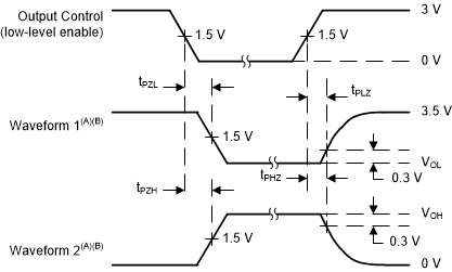
A. The outputs are measured one at a time with one transition per
measurement.
B. Waveform 1 is for an output with internal conditions such that the output
is low except when disabled by the output control. Waveform 2 is for an
output with internal conditions such that the output is high except when
disabled by the output control.
Figure 7-6 Voltage waveformsEnable and disable times, 3-state outputs