JAJSGR5B August   2009  – January 2019 SN74CBTLV1G125-Q1

PRODUCTION DATA.  

  1. 特長
  2. アプリケーション
  3. 概要
    1.     Device Images
      1.      アプリケーション回路図
  4. 改訂履歴
  5. Pin Configuration and Functions
    1.     Pin Functions
  6. Specifications
    1. 6.1 Absolute Maximum Ratings
    2. 6.2 ESD Ratings
    3. 6.3 Recommended Operating Conditions
    4. 6.4 Thermal Information
    5. 6.5 Electrical Characteristics
    6. 6.6 Switching Characteristics
  7. Parameter Measurement Information
  8. Detailed Description
    1. 8.1 Overview
    2. 8.2 Functional Block Diagram
    3. 8.3 Feature Description
    4. 8.4 Device Functional Modes
  9. Application and Implementation
    1. 9.1 Application Information
    2. 9.2 Typical Application
      1. 9.2.1 Design Requirements
      2. 9.2.2 Detailed Design Procedure
  10. 10Power Supply Recommendations
  11. 11Layout
    1. 11.1 Layout Guidelines
    2. 11.2 Layout Example
  12. 12デバイスおよびドキュメントのサポート
    1. 12.1 デバイス・サポート
    2. 12.2 ドキュメントの更新通知を受け取る方法
    3. 12.3 コミュニティ・リソース
    4. 12.4 商標
    5. 12.5 静電気放電に関する注意事項
    6. 12.6 Glossary
  13. 13メカニカル、パッケージ、および注文情報

パッケージ・オプション

メカニカル・データ(パッケージ|ピン)
サーマルパッド・メカニカル・データ
発注情報

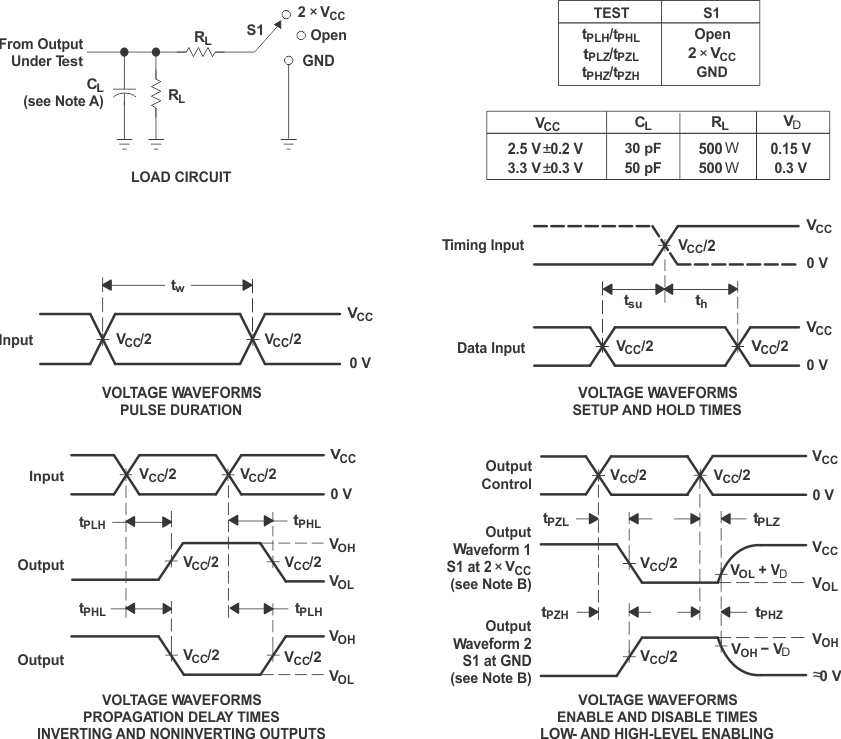
Parameter Measurement Information

SN74CBTLV1G125-Q1 pmi_cds057.gif
CL includes probe and jig capacitance.
Waveform 1 is for an output with internal conditions such that the output is low, except when disabled by the output control.
Waveform 2 is for an output with internal conditions such that the output is high, except when disabled by the output control.
All input pulses are supplied by generators having the following characteristics: PRR ≤ 10 MHz, ZO = 50 Ω, tr ≤ 2 ns,
tf ≤ 2 ns.
The outputs are measured one at a time, with one transition per measurement.
tPLZ and tPHZ are the same as tdis.
tPZL and tPZH are the same as ten.
tPLH and tPHL are the same as tpd.
All parameters and waveforms are not applicable to all devices.
Figure 1. Load Circuit and Voltage Waveforms