JAJSNM0A July 2022 – December 2022 SN74LV165A-Q1
PRODUCTION DATA
- 1 特長
- 2 アプリケーション
- 3 概要
- 4 Revision History
- 5 Pin Configuration and Functions
-
6 Specifications
- 6.1 Absolute Maximum Ratings
- 6.2 ESD Ratings
- 6.3 Recommended Operating Conditions
- 6.4 Thermal Information
- 6.5 Electrical Characteristics
- 6.6 Timing Requirements, VCC = 2.5 V ± 0.2 V
- 6.7 Timing Requirements, VCC = 3.3 V ± 0.3 V
- 6.8 Timing Requirements, VCC = 5 V ± 0.5 V
- 6.9 Switching Characteristics, VCC = 2.5 V ± 0.2 V
- 6.10 Switching Characteristics, VCC = 3.3 V ± 0.3 V
- 6.11 Switching Characteristics, VCC = 5 V ± 0.5 V
- 6.12 Operating Characteristics
- 6.13 Typical Characteristics
- 7 Parameter Measurement Information
- 8 Detailed Description
- 9 Application and Implementation
- 10Power Supply Recommendations
- 11レイアウト
- 12Device and Documentation Support
- 13Mechanical, Packaging, and Orderable Information
パッケージ・オプション
メカニカル・データ(パッケージ|ピン)
- BQB|16
サーマルパッド・メカニカル・データ
- BQB|16
発注情報
6.8 Timing Requirements, VCC = 5 V ± 0.5 V
over recommended operating free-air temperature range (unless otherwise noted) (see Figure 7-1)
| PARAMETER | TEST CONDITION | 25°C | –40°C to 125°C | UNIT | |||
|---|---|---|---|---|---|---|---|
| MIN | MAX | MIN | MAX | ||||
| tw | Pulse duration | CLK high or low | 4 | 4 | ns | ||
| SH/ LD low | 5 | 6 | |||||
| tsu | Setup time | SH/ LD high before CLK↑ | 4 | 4 | ns | ||
| SER before CLK↑ | 4 | 4 | |||||
| CLK INH before CLK↑ | 3.5 | 3.5 | |||||
| Data before SH/ LD↑ | 5 | 5 | |||||
| th | Hold time | SER data after CLK↑ | 0.5 | 0.5 | ns | ||
| Parallel data after SH/ LD↑ | 1 | 1 | |||||
| SH/ LD high after CLK↑ | 0.5 | 0.5 | |||||
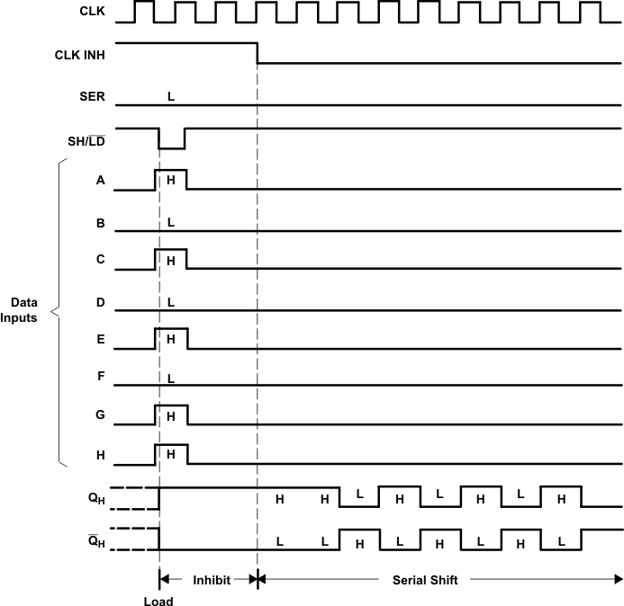
 Figure 6-1 Typical Shift, Load, and Inhibit Sequences