SCES222Q April 1999 – June 2017 SN74LVC1G86
PRODUCTION DATA.
- 1 Features
- 2 Applications
- 3 Description
- 4 Revision History
- 5 Pin Configuration and Functions
- 6 Specifications
- 7 Parameter Measurement Information
- 8 Detailed Description
- 9 Application and Implementation
- 10Power Supply Recommendations
- 11Layout
- 12Device and Documentation Support
- 13Mechanical, Packaging, and Orderable Information
パッケージ・オプション
デバイスごとのパッケージ図は、PDF版データシートをご参照ください。
メカニカル・データ(パッケージ|ピン)
- DBV|5
- DCK|5
- DRL|5
- YZP|5
サーマルパッド・メカニカル・データ
発注情報
11 Layout
11.1 Layout Guidelines
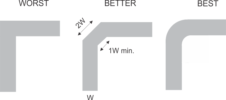
Even low data rate digital signals can have high frequency signal components due to fast edge rates. When a PCB trace turns a corner at a 90° angle, a reflection can occur. A reflection occurs primarily because of the change of width of the trace. At the apex of the turn, the trace width increases to 1.414 times the width. This increase upsets the transmission-line characteristics, especially the distributed capacitance and self–inductance of the trace which results in the reflection. Not all PCB traces can be straight and therefore some traces must turn corners. Figure 6 shows progressively better techniques of rounding corners. Only the last example (BEST) maintains constant trace width and minimizes reflections.
11.2 Layout Example
 Figure 6. Trace Example