SCES193N April 1999 – January 2015 SN74LVC2G00
PRODUCTION DATA.
- 1 Features
- 2 Applications
- 3 Description
- 4 Simplified Schematic
- 5 Revision History
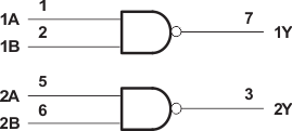
- 6 Pin Configuration and Functions
- 7 Specifications
- 8 Parameter Measurement Information
- 9 Detailed Description
- 10Application and Implementation
- 11Power Supply Recommendations
- 12Layout
- 13Device and Documentation Support
- 14Mechanical, Packaging, and Orderable Information
パッケージ・オプション
デバイスごとのパッケージ図は、PDF版データシートをご参照ください。
メカニカル・データ(パッケージ|ピン)
- DCU|8
- YZP|8
- DCT|8
サーマルパッド・メカニカル・データ
発注情報
9 Detailed Description
9.1 Overview
The SN74LVC2G00 device contains two 2-input positive-NAND gates and performs the Boolean function
Y = A × B or Y = A + B on each gate. This device is fully specified for partial-power-down applications using Ioff. The Ioff circuitry disables the outputs, preventing damaging current backflow through the device when it is powered down.
9.2 Functional Block Diagram
9.3 Feature Description
- Wide operating voltage range.
- Operates from 1.65 V to 5.5 V
- Allows down voltage translation
- Inputs accept voltages to 5.5 V
- Ioff feature
- Allows voltages on the inputs and outputs, when VCC is 0 V
9.4 Device Functional Modes
Table 1. Function Table (Each Gate)
| INPUTS | OUTPUT Y |
|
|---|---|---|
| A | B | |
| H | H | L |
| L | X | H |
| X | L | H |