SCES381N January 2002 – January 2015 SN74LVC2G17 , SN74LVC2G17
PRODUCTION DATA.
- 1 Features
- 2 Applications
- 3 Simplified Schematic
- 4 Revision History
- 5 Pin Configuration and Functions
- 6 Specifications
- 7 Parameter Measurement Information
- 8 Detailed Description
- 9 Application and Implementation
- 10Power Supply Recommendations
- 11Layout
- 12Device and Documentation Support
- 13Mechanical, Packaging, and Orderable Information
パッケージ・オプション
メカニカル・データ(パッケージ|ピン)
サーマルパッド・メカニカル・データ
- DRY|6
発注情報
9 Application and Implementation
NOTE
Information in the following applications sections is not part of the TI component specification, and TI does not warrant its accuracy or completeness. TI’s customers are responsible for determining suitability of components for their purposes. Customers should validate and test their design implementation to confirm system functionality.
9.1 Application Information
The SN74LVC2G17 device contains two buffers and performs the Boolean function Y = A. The device functions as two independent buffers, but because of Schmitt action, it may have different input threshold levels for positive-going (VT+) and negative-going (VT–) signals.
9.2 Typical Power Button Circuit
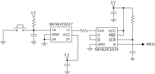 Figure 4. Device Power Button Circuit
9.2.1 Design Requirements
This device uses CMOS technology and has balanced output drive. Care should be taken to avoid bus contention because it can drive currents that would exceed maximum limits. Outputs can be combined to produce higher drive but the high drive will also create faster edges into light loads so routing and load conditions should be considered to prevent ringing.
9.2.2 Detailed Design Procedure
- Recommended Input Conditions:
- For rise time and fall time specifications, see (Δt/ΔV) in Recommended Operating Conditions table.
- For specified high and low levels, see (VIH and VIL) in Recommended Operating Conditions table.
- Inputs are overvoltage tolerant allowing them to go as high as 5.5 V at any valid VCC.
- Recommend Output Conditions:
- Load currents should not exceed 50 mA per output and 100 mA total for the part.
- Series resistors on the output may be used if the user desires to slow the output edge signal or limit the output current.
9.2.3 Application Curves
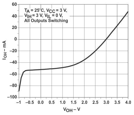 Figure 5. Output Current Drive
vs HIGH-level Output Voltage
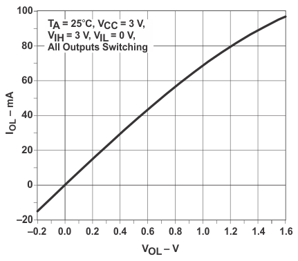 Figure 6. Output Current Drive
vs LOW-level Output Voltage