JAJSUH1 April 2024 TAS2505A-Q1
PRODUCTION DATA
- 1
- 1 特長
- 2 アプリケーション
- 3 概要
- 4 Pin Configuration and Functions
-
5 Specifications
- 5.1 Absolute Maximum Ratings
- 5.2 ESD Ratings
- 5.3 Recommended Operating Conditions
- 5.4 Thermal Information
- 5.5 Electrical Characteristics
- 5.6 I2S/LJF/RJF Timing in Master Mode
- 5.7 I2S/LJF/RJF Timing in Slave Mode
- 5.8 DSP Timing in Master Mode
- 5.9 DSP Timing in Slave Mode
- 5.10 I2C Interface Timing
- 5.11 SPI Interface Timing
- 5.12 Typical Characteristics
- 6 Parameter Measurement Information
-
7 Detailed Description
- 7.1 Overview
- 7.2 Functional Block Diagram
- 7.3 Feature Description
- 7.4 Device Functional Modes
- 7.5 Register Map
- 8 Register Map
- 9 Application and Implementation
- 10Device and Documentation Support
- 11Revision History
- 12Mechanical, Packaging, and Orderable Information
パッケージ・オプション
メカニカル・データ(パッケージ|ピン)
- RGE|24
サーマルパッド・メカニカル・データ
- RGE|24
発注情報
5.11 SPI Interface Timing
At 25°C, DVDD = 1.8V
| PARAMETER | TEST CONDITION | IOVDD=1.8V | IOVDD=3.3V | UNIT | |||||
|---|---|---|---|---|---|---|---|---|---|
| MIN | TYP | MAX | MIN | TYP | MAX | ||||
| tsck | SCLK period (1) | 100 | 50 | ns | |||||
| tsckh | SCLK pulse width High | 50 | 25 | ns | |||||
| tsckl | SCLK pulse width Low | 50 | 25 | ns | |||||
| tlead | Enable lead time | 30 | 20 | ns | |||||
| tlag | Enable lag time | 30 | 20 | ns | |||||
| td | Sequential transfer delay | 40 | 20 | ns | |||||
| ta | Slave DOUT access time | 40 | 40 | ns | |||||
| tdis | Slave DOUT disable time | 40 | 40 | ns | |||||
| tsu | DIN data setup time | 15 | 15 | ns | |||||
| thi | DIN data hold time | 15 | 10 | ns | |||||
| tv;DOUT | DOUT data valid time | 25 | 18 | ns | |||||
| tr | SCLK rise time | 4 | 4 | ns | |||||
| tf | SCLK fall time | 4 | 4 | ns | |||||
(1) These parameters are based on characterization and are not tested in production.
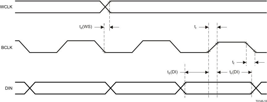 Figure 5-1 I2S/LJF/RJF Timing in Master Mode
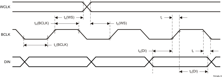 Figure 5-2 I2S/LJF/RJF Timing in Slave Mode
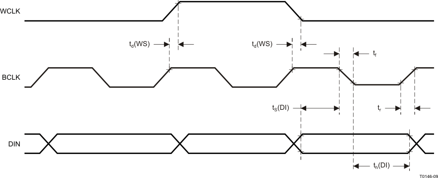 Figure 5-3 DSP Timing in Master Mode
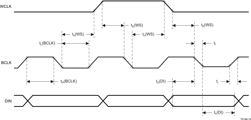 Figure 5-4 DSP Timing in Slave Mode
 Figure 5-5 I2C Interface Timing
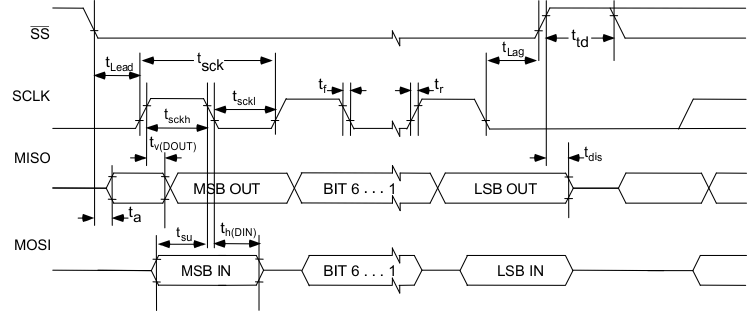 Figure 5-6 SPI Interface Timing Diagram