SLAS844A May 2012 – January 2016 TAS5624A
PRODUCTION DATA.
- 1 Features
- 2 Applications
- 3 Description
- 4 Revision History
- 5 Device Comparison Table
- 6 Pin Configuration and Functions
-
7 Specifications
- 7.1 Absolute Maximum Ratings
- 7.2 ESD Ratings
- 7.3 Recommended Operating Conditions
- 7.4 Thermal Information
- 7.5 Electrical Characteristics
- 7.6 Electrical Characteristics - Audio Specification Stereo (BTL)
- 7.7 Electrical Characteristics - Audio Specification 4 Channels (SE)
- 7.8 Electrical Characteristics - Audio Specification Mono (PBTL)
- 7.9 Typical Characteristics
- 8 Parameter Measurement Information
-
9 Detailed Description
- 9.1 Overview
- 9.2 Functional Block Diagrams
- 9.3
Feature Description
- 9.3.1 System Power-Up and Power-Down Sequence
- 9.3.2 Start-Up and Shutdown Ramp Sequence
- 9.3.3 Unused Output Channels
- 9.3.4 Device Protection System
- 9.3.5 Pin-to-Pin Short-Circuit Protection (PPSC)
- 9.3.6 Overtemperature Protection
- 9.3.7 Overtemperature Warning, OTW
- 9.3.8 Undervoltage Protection (UVP) and Power-On Reset (POR)
- 9.3.9 Error Reporting
- 9.3.10 Fault Handling
- 9.3.11 Device Reset
- 9.3.12 System Design Consideration
- 9.4 Device Functional Modes
- 10Application and Implementation
- 11Power Supply Recommendations
- 12Layout
- 13Device and Documentation Support
- 14Mechanical, Packaging, and Orderable Information
パッケージ・オプション
メカニカル・データ(パッケージ|ピン)
- DDV|44
サーマルパッド・メカニカル・データ
- DDV|44
発注情報
9 Detailed Description
9.1 Overview
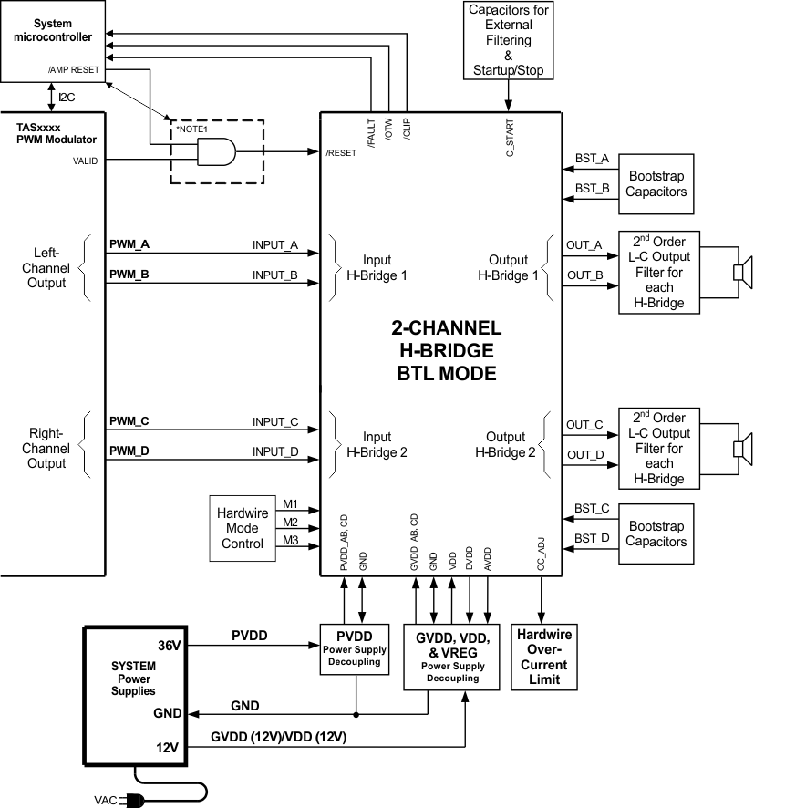
TAS5624A is a PWM input, audio PWM (class-D) amplifier. the output of the TAS5624A can be configured for single-ended, bridge-tied load (BTL) or parallel BTL (PBTL) output. It requires two railes for power supply, PVDD and 12 V (GVDD and VDD). Figure 13 shows typical connections for BTL outputs. A detailed schematic can be viewed in TAS5624A EVM User's Guide (SLAU376).
9.2 Functional Block Diagrams

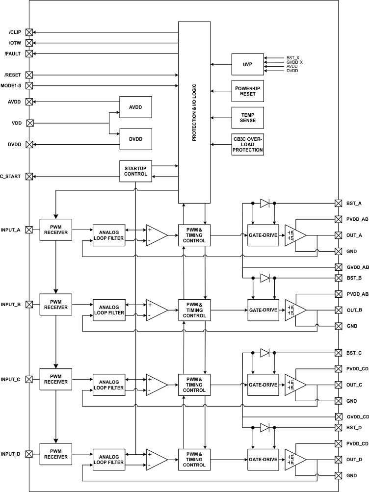
 Figure 14. Functional Block Diagram
9.3 Feature Description
9.3.1 System Power-Up and Power-Down Sequence
9.3.1.1 Powering Up
The TAS5624A does not require a power-up sequence. The outputs of the H-bridges remain in a high-impedance state until the gate-drive supply voltage (GVDD_X) and VDD voltage are above the undervoltage protection (UVP) voltage threshold (see the Electrical Characteristics table of this data sheet). Although not specifically required, TI recommends to hold RESET in a low state while powering up the device. This allows an internal circuit to charge the external bootstrap capacitors by enabling a weak pulldown of the half-bridge output.
9.3.1.2 Powering Down
The TAS5624A does not require a power-down sequence. The device remains fully operational as long as the gate-drive supply (GVDD_X) voltage and VDD voltage are above the undervoltage protection (UVP) voltage threshold (see the Electrical Characteristics table of this data sheet). Although not specifically required, it is a good practice to hold RESET low during power down, thus preventing audible artifacts including pops or clicks.
9.3.2 Start-Up and Shutdown Ramp Sequence
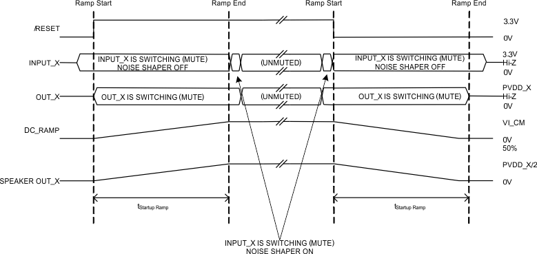
The integrated start-up and stop sequence ensures a click-free and pop-free start-up and shutdown sequence of the amplifier. The start-up sequence uses a voltage ramp with a duration set by the CSTART capacitor. The sequence uses the input PWM signals to generate output PWM signals, hence input idle PWM must be present during both start-up and shutdown ramping sequences.
VDD, GVDD_X and PVDD_X power supplies must be turned on and with settled outputs before starting
the start-up ramp by setting RESET high.
During start-up and shutdown ramp, the input PWM signals must be in muted condition with the PWM processor noise shaper activity turned off (50% duty cycle).
The duration of the start-up and shutdown ramp is 100 ms + X ms, where X is the CSTART capacitor value in nF.
TI recommends using a 100-nF CSTART in BTL and PBTL mode and 1 µF in SE mode configuration. This results in ramp times of 200 ms and 1.1 s respectively. The longer ramp time in SE configuration allows charge and discharge of the output AC-coupling capacitor without audible artifacts.
 Figure 15. Start-Up and Shutdown Ramp
9.3.3 Unused Output Channels
If all available output channels are not used, TI recommends disabling of unused output nodes to reduce power consumption. Furthermore by disabling unused output channels the cost of unused output LC demodulation filters can be avoided.
Disabling a channel is done by leave the bootstrap capacitor (BST) unstuffed and connecting the respective input to GND. The unused output pins can be left floating.
NOTE
The PVDD decoupling capacitors must still be mounted.
Table 1. Unused Output Channels
| OPERATING MODE | PWM INPUT | OUTPUT CONFIGURATION | UNUSED CHANNEL | INPUT_A | INPUT_B | INPUT_C | INPUT_D | UNSTUFFED COMPONENT |
|---|---|---|---|---|---|---|---|---|
| 000 | 2N + 1 | 2 × BTL | AB CD |
GND PWMa |
GND PWMb |
PWMc GND |
PWMd GND |
BST_A & BST_B capacitor BST_C & BST_D capacitor |
| 001 | 1N + 1 | |||||||
| 010 | 2N + 1 | |||||||
| 101 | 1N + 1 | 4 × SE | A | GND | PWMb | PWMc | PWMd | BST_A capacitor |
| B | PWMa | GND | PWMc | PWMd | BST_B capacitor | |||
| C | PWMa | PWMb | GND | PWMd | BST_C capacitor | |||
| D | PWMa | PWMb | PWMc | GND | BST_D capacitor |
9.3.4 Device Protection System
The TAS5624A contains advanced protection circuitry carefully designed to facilitate system integration and ease of use, as well as to safeguard the device from permanent failure due to a wide range of fault conditions such as short circuits, overload, overtemperature, and undervoltage. The TAS5624A responds to a fault by immediately setting the power stage in a high-impedance (Hi-Z) state and asserting the FAULT pin low. In situations other than overload and overtemperature error (OTE), the device automatically recovers when the fault condition has been removed, that is, the supply voltage has increased.
The device will function on errors, as shown in Table 2.
Table 2. Device Protection
| BTL MODE | PBTL MODE | SE MODE | |||
|---|---|---|---|---|---|
| CHANNEL FAULT | TURNS OFF | CHANNEL FAULT | TURNS OFF | CHANNEL FAULT | TURNS OFF |
| A | A + B | A | A + B + C + D | A | A + B |
| B | B | B | |||
| C | C + D | C | C | C + D | |
| D | D | D | |||
Bootstrap UVP does not shutdown according to the table, it shuts down the respective high-side FET.
9.3.5 Pin-to-Pin Short-Circuit Protection (PPSC)
The PPSC detection system protects the device from permanent damage if a power output pin (OUT_X) is shorted to GND or PVDD_X. For comparison, the OC protection system detects an overcurrent after the demodulation filter where PPSC detects shorts directly at the pin before the filter. PPSC detection is performed at start-up, for example, when VDD is supplied, consequently a short to either GND or PVDD_X after system start-up does not activate the PPSC detection system. When PPSC detection is activated by a short on the output, all half-bridges are kept in a Hi-Z state until the short is removed, the device then continues the start-up sequence and starts switching. The detection is controlled globally by a two-step sequence. The first step ensures that there are no shorts from OUT_X to GND, the second step tests that there are no shorts from OUT_X to PVDD_X. The total duration of this process is roughly proportional to the capacitance of the output LC filter. The typical duration is < 15 ms/μF. While the PPSC detection is in progress, FAULT is kept low, and the device will not react to changes applied to the RESET pins. If no shorts are present the PPSC detection passes, and FAULT is released. A device reset will not start a new PPSC detection. PPSC detection is enabled in BTL and PBTL output configurations, the detection is not performed in SE mode. To make sure not to trip the PPSC detection system, TI recommends not to insert resistive load to GND or PVDD_X.
9.3.6 Overtemperature Protection
The TAS5624A has a two-level, temperature-protection system that asserts an active-low warning signal (OTW) when the device junction temperature exceeds 125°C (typical). If the device junction temperature exceeds 155°C (typical), the device is put into thermal shutdown, resulting in all half-bridge outputs being set in the high-impedance (Hi-Z) state and FAULT being asserted low. OTE is latched in this case. To clear the OTE latch, RESET must be asserted. Thereafter, the device resumes normal operation.
9.3.7 Overtemperature Warning, OTW
The overtemperature warning OTW asserts when the junction temperature has exceeded recommended operating temperature. Operation at junction temperatures above OTW threshold is exceeding recommended operation conditions and is strongly advised to avoid.
If OTW asserts, take action to reduce power dissipation to allow junction temperature to decrease until it gets below the OTW hysteresis threshold. This action can be decreasing audio volume or turning on a system cooling fan.
9.3.8 Undervoltage Protection (UVP) and Power-On Reset (POR)
The UVP and POR circuits of the TAS5624A fully protect the device in any power-up, power-down, or brownout situation. While powering up, the POR circuit resets the overload circuit (OLP) and ensures that all circuits are fully operational when the GVDD_X and VDD supply voltages reach stated in the Electrical Characteristics table. Although GVDD_X and VDD are independently monitored, a supply voltage drop below the UVP threshold on any VDD or GVDD_X pin results in all half-bridge outputs immediately being set in the high-impedance (Hi-Z) state and FAULT being asserted low. The device automatically resumes operation when all supply voltages have increased above the UVP threshold.
9.3.9 Error Reporting
NOTE
Asserting RESET low forces the FAULT signal high, independent of faults being present.
TI recommends monitoring the OTW signal using the system microcontroller and responding to an overtemperature warning signal by, for example, turning down the volume to prevent further heating of the device resulting in device shutdown (OTE).
To reduce external component count, an internal pullup resistor to 3.3 V is provided on FAULT, CLIP, and OTW outputs. See Electrical Characteristics table for actual values.
The FAULT and OTW pins are active-low, open-drain outputs. Their function is for protection-mode signaling to a PWM controller or other system-control device.
Any fault resulting in device shutdown is signaled by the FAULT pin going low. Likewise, OTW goes low when the device junction temperature exceeds 125°C (see Table 3).
Table 3. Error Reporting
| FAULT | OTW | DESCRIPTION | |
|---|---|---|---|
| 0 | 0 | Overtemperature (OTE) or overload (OLP) or undervoltage (UVP) | |
| 0 | 1 | Overload (OLP) or undervoltage (UVP) | |
| 1 | 0 | Junction temperature higher than 125°C (overtemperature warning) | |
| 1 | 1 | Junction temperature lower than 125°C and no OLP or UVP faults (normal operation) | |
9.3.10 Fault Handling
If a fault situation occurs while in operation, the device will act accordingly to the fault being a global or a channel fault. A global fault is a chip-wide fault situation and causes all PWM activity of the device to shut down, and will assert FAULT low. A global fault is a latching fault and clearing FAULT and restart operation requires resetting the device by toggling RESET. Toggling RESET must never be allowed with excessive system temperature, so it is advised to monitor RESET by a system microcontroller and only allow releasing RESET (RESET high) if the OTW signal is cleared (high). A channel fault will result in shutdown of the PWM activity of the affected channels. Asserting RESET low forces the FAULT signal high, independent of faults being present. TI recommends monitoring the OTW signal using the system microcontroller and responding to an overtemperature warning signal by, for example, turning down the volume to prevent further heating of the device resulting in device shutdown (OTE).
Table 4. Fault Handling
| FAULT AND EVENT | FAULT AND EVENT DESCRIPTION |
GLOBAL OR CHANNEL |
REPORTING METHOD | LATCHED AND SELF CLEARING |
ACTION NEEDED TO CLEAR | OUTPUT FETs |
|---|---|---|---|---|---|---|
| PVDD_X UVP | Voltage Fault | Global | FAULT Pin | Self-Clearing | Increase affected supply voltage | Hi-Z |
| VDD UVP | ||||||
| GVDD_X UVP | ||||||
| AVDD UVP | ||||||
| POR (DVDD UVP) | Power On Reset | Global | FAULT Pin | Self-Clearing | Allow DVDD to rise | H-Z |
| BST UVP | Voltage Fault | Channel (half-bridge) |
None | Self-Clearing | Allow BST cap to recharge (lowside on, VDD 12 V) |
HighSide Off |
| OTW | Thermal Warning | Global | OTW Pin | Self-Clearing | Cool below lower OTW threshold | Normal operation |
| OTE (OTSD) | Thermal Shutdown | Global | FAULT Pin | Latched | Toggle RESET | Hi-Z |
| OLP (CBC > 2.6ms) | OC shutdown | Channel | FAULT Pin | Latched | Toggle RESET | Hi-Z |
| Latched OC (ROC > 47k) | OC shutdown | Channel | FAULT Pin | Latched | Toggle RESET | Hi-Z |
| CBC (24k < ROC < 33k) | OC Limiting | Channel | None | Self-Clearing | Reduce signal level or remove short | Flip state, cycle by cycle at fs / 2 |
| Stuck at Fault(1)
(1 to 3 channels) |
No PWM | Channel | None | Self-Clearing | Resume PWM | Hi-Z |
| Stuck at Fault(1)
(All channels) |
No PWM | Global | None | Self-Clearing | Resume PWM | Hi-Z |
9.3.11 Device Reset
When RESET is asserted low, all power-stage FETs in the four half-bridges are forced into a high-impedance (Hi-Z) state.
In BTL modes, to accommodate bootstrap charging prior to switching start, asserting the reset input low enables weak pulldown of the half-bridge outputs. In the SE mode, the output is forced into a high impedance state when asserting the reset input low. Asserting reset input low removes any fault information to be signaled on the FAULT output, that is, FAULT is forced high. A rising-edge transition on reset input allows the device to resume operation after an overload fault. To ensure thermal reliability, the rising edge of RESET must occur no sooner than 4 ms after the falling edge of FAULT.
9.3.12 System Design Consideration
A rising-edge transition on RESET input allows the device to execute the start-up sequence and starts switching.
Apply audio only according to the timing information for start-up and shutdown sequence. That will start and stop the amplifier without audible artifacts in the output transducers.
The CLIP signal indicates that the output is approaching clipping (when output PWM starts skipping pulses due to loop filter saturation). The signal can be used to initiate an audio volume decrease or to adjust the power supply rail.
The device inverts the audio signal from input to output.
The DVDD and AVDD pins are not recommended to be used as a voltage source for external circuitry.
9.4 Device Functional Modes
There are three main output modes that the user can configure the device as per application requirement. In addition, there are two PWM modulation modes, AD and BD. AD modulation can have single-ended (SE) or differential analog inputs. AD modulation can also be configured to have SE, BTL, BTL + SE, or PBTL outputs. BD modulation requires differential analog inputs. BD modulation can only be configured in BTL or PBTL mode.