SLOS670B November 2010 – December 2016 TAS5727
PRODUCTION DATA.
- 1 Features
- 2 Applications
- 3 Description
- 4 Revision History
- 5 Description (continued)
- 6 Device Comparison Table
- 7 Pin Configuration and Functions
-
8 Specifications
- 8.1 Absolute Maximum Ratings
- 8.2 ESD Ratings
- 8.3 Recommended Operating Conditions
- 8.4 Thermal Information
- 8.5 DC Electrical Characteristics
- 8.6 AC Electrical Characteristics (BTL, PBTL)
- 8.7 PLL Input Parameters and External Filter Components
- 8.8 Serial Audio Ports Slave Mode
- 8.9 I2C Serial Control Port Operation
- 8.10 Reset Timing (RESET)
- 8.11 Typical Characteristics
- 9 Parameter Measurement Information
-
10Detailed Description
- 10.1 Overview
- 10.2 Functional Block Diagrams
- 10.3
Feature Description
- 10.3.1 Power Supply
- 10.3.2 I2C Address Selection and Fault Output
- 10.3.3 Device Protection Systems
- 10.3.4 Clock, Auto Detection, and PLL
- 10.3.5 PWM Section
- 10.3.6 SSTIMER Functionality
- 10.3.7 Single-Filter PBTL Mode
- 10.3.8 I2C Serial Control Interface
- 10.3.9 Audio Serial Interface
- 10.3.10 Serial Interface Control and Timing
- 10.3.11 Dynamic Range Control (DRC)
- 10.3.12 PWM Level Meter
- 10.4 Device Functional Modes
- 10.5 Programming
- 10.6
Register Maps
- 10.6.1 Clock Control Register (0x00)
- 10.6.2 Device Id Register (0x01)
- 10.6.3 Error Status Register (0x02)
- 10.6.4 System Control Register 1 (0x03)
- 10.6.5 Serial Data Interface Register (0x04)
- 10.6.6 System Control Register 2 (0x05)
- 10.6.7 Soft Mute Register (0x06)
- 10.6.8 Volume Registers (0x07, 0x08, 0x09)
- 10.6.9 Volume Configuration Register (0x0E)
- 10.6.10 Modulation Limit Register (0x10)
- 10.6.11 Interchannel Delay Registers (0x11, 0x12, 0x13, and 0x14)
- 10.6.12 PWM Shutdown Group Register (0x19)
- 10.6.13 Start/Stop Period Register (0x1A)
- 10.6.14 Oscillator Trim Register (0x1B)
- 10.6.15 BKND_ERR Register (0x1C)
- 10.6.16 Input Multiplexer Register (0x20)
- 10.6.17 Channel 4 Source Select Register (0x21)
- 10.6.18 PWM Output MUX Register (0x25)
- 10.6.19 DRC Control Register (0x46)
- 10.6.20 PWM Switching Rate Control Register (0x4F)
- 10.6.21 Bank Switch and EQ Control (0x50)
-
11Application and Implementation
- 11.1 Application Information
- 11.2
Typical Applications
- 11.2.1 Stereo Stereo Bridge Tied Load Application
- 11.2.2 Mono Parallel Bridge Tied Load Application
- 12Power Supply Recommendations
- 13Layout
- 14Device and Documentation Support
- 15Mechanical, Packaging, and Orderable Information
パッケージ・オプション
メカニカル・データ(パッケージ|ピン)
- PHP|48
サーマルパッド・メカニカル・データ
- PHP|48
発注情報
13 Layout
13.1 Layout Guidelines
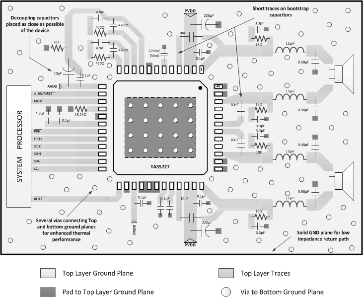
Class-D switching edges are fast and switched currents are high, so it is necessary to take care when planning the layout of the printed-circuit board. The following suggestions helps meet audio, thermal, and EMC requirements.
- TAS5727 uses the PCB for heat sinking; therefore, the PowerPAD™ needs to be soldered to the PCB and adequate copper area and copper vias connecting the top, bottom and internal layers should be used.
- Decoupling capacitors: the high-frequency decoupling capacitors should be placed as close to the supply pins as possible; on the TAS5727, a 1-µF high-quality ceramic capacitor is used. Large (10-μF or greater) bulk power supply decoupling capacitors should be placed near the TAS5727 on the PVDD supplies.
- Keep the current loop from each of the outputs through the output inductor and the small filter capacitor and back to GND as small and tight as possible. The size of this current loop determines its effectiveness as an antenna.
- Grounding: TI recommends a big common GND plane. The PVDD decoupling capacitors should connect to GND. The TAS5727 PowerPAD should be connected to GND.
- Output filter: remember to select inductors that can handle the high short-circuit current of the device. The LC filter should be placed close to the outputs.
The EVM product folder and User’s Guide available on www.ti.com shows schematic, bill of material, gerber files, and more detailed layout plots.
13.2 Layout Example
 Figure 46. Layout Example