JAJSFN8A June   2018  – February 2022 TCA9517-Q1

PRODUCTION DATA  
  1. 特長
  2. アプリケーション
  3. 概要
  4. Revision History
  5. 概要 (続き)
  6. Pin Configuration and Functions
  7. Specifications
    1. 7.1 Absolute Maximum Ratings
    2. 7.2 ESD Ratings
    3. 7.3 Recommended Operating Conditions
    4. 7.4 Thermal Information
    5. 7.5 Electrical Characteristics
    6. 7.6 Timing Requirements
    7. 7.7 I2C Interface Switching Characteristics
    8. 7.8 Typical Characteristics
  8. Parameter Measurement Information
  9. Detailed Description
    1. 9.1 Overview
    2. 9.2 Functional Block Diagram
    3. 9.3 Feature Description
      1. 9.3.1 Two-Channel Bidirectional Buffer
      2. 9.3.2 Active-High Repeater-Enable Input
      3. 9.3.3 VOL B-Side Offset Voltage
      4. 9.3.4 Standard Mode and Fast Mode Support
      5. 9.3.5 Clock Stretching Support
    4. 9.4 Device Functional Modes
  10. 10Application and Implementation
    1. 10.1 Application Information
    2. 10.2 Typical Application
      1. 10.2.1 Design Requirements
      2. 10.2.2 Detailed Design Procedure
        1. 10.2.2.1 Clock Stretching Support
        2. 10.2.2.2 VILC and Pullup Resistor Sizing
      3. 10.2.3 Application Curve
  11. 11Power Supply Recommendations
  12. 12Layout
    1. 12.1 Layout Guidelines
    2. 12.2 Layout Example
  13. 13Device and Documentation Support
    1. 13.1 Device Support
    2. 13.2 Receiving Notification of Documentation Updates
    3. 13.3 サポート・リソース
    4. 13.4 Trademarks
    5. 13.5 Electrostatic Discharge Caution
    6. 13.6 Glossary

パッケージ・オプション

メカニカル・データ(パッケージ|ピン)
サーマルパッド・メカニカル・データ
発注情報

Application Curve

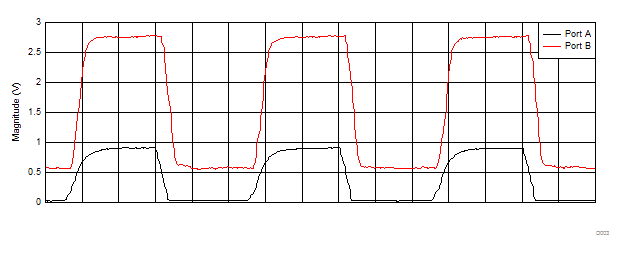
GUID-4622AEE9-D77D-4171-A6E7-75B8B09526AB-low.gifFigure 10-6 Voltage Translation at 400 kHz, VCCA = 0.9 V, VCCB = 2.7 V