SCPS242D December 2012 – July 2017 TCA9517
PRODUCTION DATA.
- 1 Features
- 2 Applications
- 3 Description
- 4 Revision History
- 5 Description (continued)
- 6 Pin Configuration and Functions
- 7 Specifications
- 8 Parameter Measurement Information
- 9 Detailed Description
- 10Application and Implementation
- 11Power Supply Recommendations
- 12Layout
- 13Device and Documentation Support
- 14Mechanical, Packaging, and Orderable Information
パッケージ・オプション
メカニカル・データ(パッケージ|ピン)
サーマルパッド・メカニカル・データ
発注情報
10 Application and Implementation
NOTE
Information in the following applications sections is not part of the TI component specification, and TI does not warrant its accuracy or completeness. TI’s customers are responsible for determining suitability of components for their purposes. Customers should validate and test their design implementation to confirm system functionality.
10.1 Application Information
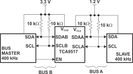
A typical application is shown in Figure 7. In this example, the system master is running on a 3.3 V I2C bus, and the slave is connected to a 1.2 V I2C bus. Both buses run at 400 kHz. Master devices can be placed on either bus.
The TCA9517 is 5-V tolerant, so it does not require any additional circuitry to translate between 0.9 V to 5.5 V bus voltages and 2.7 V to 5.5 V bus voltages.
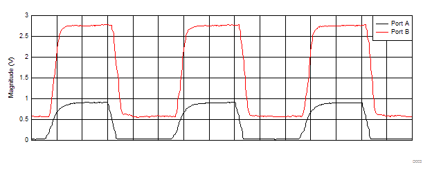
When the A side of the TCA9517 is pulled low by a driver on the I2C bus, a comparator detects the falling edge when it goes below 0.3 × VCCA and causes the internal driver on the B-side to turn on, causing the B-side to pull down to about 0.5 V. When the B-side of the TCA9517 falls, first a CMOS hysteresis-type input detects the falling edge and causes the internal driver on the A side to turn on and pull the A-side pin down to ground. In order to illustrate what would be seen in a typical application, refer to Figure 9 and Figure 10. If the bus master in Figure 7 were to write to the slave through the TCA9517 , waveforms shown in Figure 9 would be observed on the A bus. This looks like a normal I2C transmission, except that the high level may be as low as 0.9 V, and the turn on and turn off of the acknowledge signals are slightly delayed.
On the B-side bus of the TCA9517 , the clock and data lines would have a positive offset from ground equal to the VOL of the TCA9517 . After the eighth clock pulse, the data line is pulled to the VOL of the slave device, which is very close to ground in this example. At the end of the acknowledge, the level rises only to the low level set by the driver in the TCA9517 for a short delay, while the A-bus side rises above 0.3 × VCCA and then continues high.
10.2 Typical Application
 Figure 7. Typical Application Schematic
10.2.1 Design Requirements
For the level translating application, the following should be true:
- VCCA = 0.9 V to 5.5 V
- VCCB = 2.7 to 5.5 V
- B-side ports must not be connected together
10.2.2 Detailed Design Procedure
10.2.2.1 Clock Stretching Support
The TCA9517 can support clock stretching, but care needs to be taken to minimize the overshoot voltage presented during the hand-off between the slave and master. This is best done by increasing the pull-up resistor value.
10.2.2.2 VILC and Pullup Resistor Sizing
For the TCA9517 to function correctly, all devices on the B-side must be able to pull the B-side below the voltage input low contention level (VILC). This means that the VOL of any device on the B-side must be below
0.4 V.
VOL of a device can be adjusted by changing the IOL through the device which is set by the pull-up resistance value. The pull-up resistance on the B-side must be carefully selected to ensure that logic levels will be transferred correctly to the A-side.
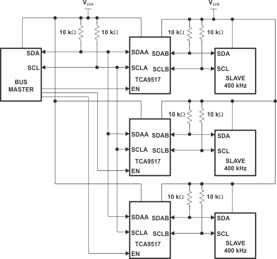
 Figure 8. Typical Star Application
Multiple A sides of TCA9517 s can be connected in a star configuration, allowing all nodes to communicate with each other.
 Figure 9. Typical Series Application
To further extend the I2C bus for long traces/cables, multiple TCA9517 s can be connected in series as long as the A-side is connected to the B-side. I2C bus slave devices can be connected to any of the bus segments. The number of devices that can be connected in series is limited by repeater delay/time-of-flight considerations on the maximum bus speed requirements.
 Figure 10. Bus A (0.9 V to 5.5 V Bus) Waveform
 Figure 11. Bus B (2.7 V to 5.5 V Bus) Waveform
10.2.3 Application Curve
 Figure 12. Voltage Translation at 400 kHz, VCCA = 0.9 V, VCCB = 2.7 V