SCPS242D December 2012 – July 2017 TCA9517
PRODUCTION DATA.
- 1 Features
- 2 Applications
- 3 Description
- 4 Revision History
- 5 Description (continued)
- 6 Pin Configuration and Functions
- 7 Specifications
- 8 Parameter Measurement Information
- 9 Detailed Description
- 10Application and Implementation
- 11Power Supply Recommendations
- 12Layout
- 13Device and Documentation Support
- 14Mechanical, Packaging, and Orderable Information
パッケージ・オプション
メカニカル・データ(パッケージ|ピン)
サーマルパッド・メカニカル・データ
発注情報
7 Specifications
7.1 Absolute Maximum Ratings
over operating free-air temperature range (unless otherwise noted)(1)| MIN | MAX | UNIT | |||
|---|---|---|---|---|---|
| VCCB | Supply voltage range | –0.5 | 7 | V | |
| VCCA | Supply voltage range | –0.5 | 7 | V | |
| VI | Enable input voltage range(2) | –0.5 | 7 | V | |
| VI/O | I2C bus voltage range(2) | –0.5 | 7 | V | |
| IIK | Input clamp current | VI < 0 | –50 | mA | |
| IOK | Output clamp current | VO < 0 | –50 | ||
| IO | Continuous output current | ±50 | mA | ||
| Continuous current through VCC or GND | ±100 | mA | |||
| Tstg | Storage temperature range | –65 | 150 | °C | |
(1) Stresses beyond those listed under Absolute Maximum Ratings may cause permanent damage to the device. These are stress ratings only, which do not imply functional operation of the device at these or any other conditions beyond those indicated under Recommended Operating Conditions. Exposure to absolute-maximum-rated conditions for extended periods may affect device reliability.
(2) The input negative-voltage and output voltage ratings may be exceeded if the input and output current ratings are observed.
7.2 ESD Ratings
| VALUE | UNIT | |||
|---|---|---|---|---|
| V(ESD) | Electrostatic discharge | Human body model (HBM), per ANSI/ESDA/JEDEC JS-001(1) | ±5500 | V |
| Charged-device model (CDM), per JEDEC specification JESD22-C101(2) | ±1000 | |||
| Machine model (A115-A) | ±200 | |||
(1) JEDEC document JEP155 states that 500 V HBM allows safe manufacturing with a standard ESD control process.
(2) JEDEC document JEP157 states that 250 V CDM allows safe manufacturing with a standard ESD control process.
7.3 Recommended Operating Conditions
| MIN | MAX | UNIT | |||
|---|---|---|---|---|---|
| VCCA | Supply voltage, A-side bus | 0.9(2) | 5.5 | V | |
| VCCB | Supply voltage, B-side bus | 2.7 | 5.5 | V | |
| VIH | High-level input voltage | SDAA, SCLA | 0.7 × VCCA | 5.5 | V |
| SDAB, SCLB | 0.7 × VCCB | 5.5 | |||
| EN | 0.7 × VCCB | 5.5 | |||
| VIL | Low-level input voltage | SDAA, SCLA | 0.3 × VCCA | V | |
| SDAB, SCLB(1) | 0.3 × VCCB | ||||
| EN | 0.3 × VCCB | ||||
| IOL | Low-level output current | 6 | mA | ||
| TA | Operating free-air temperature | –40 | 85 | °C | |
(1) VIL specification is for the first low level seen by the SDAB and SCLB lines. VILc is for the second and subsequent low levels seen by the SDAB and SCLB lines. See VILC and Pullup Resistor Sizing for VILC application information
(2) Low-level supply voltage
7.4 Thermal Information
| THERMAL METRIC(1) | TCA9517 | UNIT | ||
|---|---|---|---|---|
| DGK (VSSOP) | D (SOIC) | |||
| 8 PINS | 8 PINS | |||
| RθJA | Junction-to-ambient thermal resistance | 187.6 | 133.6 | °C/W |
| RθJC(top) | Junction-to-case (top) thermal resistance | 59.3 | 87.6 | °C/W |
| RθJB | Junction-to-board thermal resistance | 108.6 | 74.2 | °C/W |
| ψJT | Junction-to-top characterization parameter | 3.4 | 36.9 | °C/W |
| ψJB | Junction-to-board characterization parameter | 106.9 | 73.7 | °C/W |
(1) For more information about traditional and new thermal metrics, see the Semiconductor and IC Package Thermal Metrics application report, SPRA953.
7.5 Electrical Characteristics
VCCB = 2.7 V to 5.5 V, GND = 0 V, TA = –40°C to 85°C (unless otherwise noted)| PARAMETER | TEST CONDITIONS | VCCB | MIN | TYP | MAX | UNIT | ||
|---|---|---|---|---|---|---|---|---|
| VIK | Input clamp voltage | II = –18 mA | 2.7 V to 5.5 V | –1.2 | V | |||
| VOL | Low-level output voltage | SDAB, SCLB | IOL = 100 μA or 6 mA, VILA = VILB = 0 V |
2.7 V to 5.5 V | 0.45 | 0.52 | 0.6 | V |
| SDAA, SCLA | IOL = 6 mA | 0.1 | 0.2 | |||||
| VOL – VILc | Low-level input voltage below low-level output voltage | SDAB, SCLB | ensured by design | 2.7 V to 5.5 V | 70 | mV | ||
| VILC | SDA and SCL low-level input voltage contention | SDAB, SCLB | 2.7 V to 5.5 V | 0.4 | V | |||
| ICC | Quiescent supply current for VCCA | Both channels low, SDAA = SCLA = GND and SDAB = SCLB = open, or SDAA = SCLA = open and SDAB = SCLB = GND |
1 | mA | ||||
| ICC | Quiescent supply current | Both channels high, SDAA = SCLA = VCCA and SDAB = SCLB = VCCB and EN = VCCB |
5.5 V | 1.5 | 5 | mA | ||
| Both channels low, SDAA = SCLA = GND and SDAB = SCLB = open |
1.5 | 5 | ||||||
| In contention, SDAA = SCLA = GND and SDAB = SCLB = GND |
3 | 5 | ||||||
| II | Input leakage current | SDAB, SCLB | VI = VCCB | 2.7 V to 5.5 V | ±1 | μA | ||
| VI = 0.2 V | 10 | |||||||
| SDAA, SCLA | VI = VCCB | ±1 | ||||||
| VI = 0.2 V | 10 | |||||||
| EN | VI = VCCB | ±1 | ||||||
| VI = 0.2 V | –10 | –30 | ||||||
| IOH | High-level output leakage current | SDAB, SCLB | VO = 3.6 V | 2.7 V to 5.5 V | 10 | μA | ||
| SDAA, SCLA | 10 | |||||||
| CI | Input capacitance | EN | VI = 3 V or 0 V | 3.3 V | 6 | 10 | pF | |
| SCLA, SCLB | VI = 3 V or 0 V | 3.3 V | 8 | 13 | ||||
| 0 V | 7 | 11 | ||||||
| CIO | Input/output capacitance | SDAA, SDAB | VI = 3 V or 0 V | 3.3 V | 8 | 13 | pF | |
| 0 V | 7 | 11 | ||||||
7.6 Timing Requirements
over recommended operating free-air temperature range (unless otherwise noted)| MIN | MAX | UNIT | ||
|---|---|---|---|---|
| tsu | Setup time, EN high before Start condition(1) | 100 | ns | |
| th | Hold time, EN high after Stop condition(1) | 100 | ns | |
(1) EN should change state only when the global bus and the repeater port are in an idle state.
7.7 I2C Interface Switching Characteristics
VCCB = 2.7 V to 5.5 V, GND = 0 V, TA = –40°C to 85°C (unless otherwise noted)(1) (4)| PARAMETER | FROM (INPUT) |
TO (OUTPUT) |
TEST CONDITIONS | MIN | TYP(5) | MAX | UNIT | ||
|---|---|---|---|---|---|---|---|---|---|
| tPLZ | Propagation delay | SDAB, SCLB(3) (see Figure 6) | SDAA, SCLA(3) (see Figure 6) | 80 | 141 | 250 | ns | ||
| SDAA, SCLA(2) (see Figure 5) | SDAB, SCLB(2) (see Figure 5) | 25 | 74 | 110 | |||||
| tPZL | Propagation delay | SDAB, SCLB | SDAA, SCLA | VCCA ≤ 2.7 V (see Figure 4) | 30 | 76(6) | 110 | ns | |
| VCCA ≥ 3 V (see Figure 4) |
10 | 86 | 230 | ||||||
| SDAA, SCLA(2) (see Figure 5) | SDAB, SCLB(2) (see Figure 5) | 60 | 107 | 230 | |||||
| tTLH | Transition time | B-side to A side | 80% | 20% | VCCA ≤ 2.7 V (see Figure 5) |
10 | 12 | 15 | ns |
| VCCA ≥ 3 V (see Figure 5) |
40 | 42 | 45 | ||||||
| A side to B-side (see Figure 4) |
110 | 125 | 140 | ||||||
| tTHL | Transition time | B-side to A side | 80% | 20% | VCCA ≤ 2.7 V (see Figure 5) |
1 | 52(6) | 105 | ns |
| VCCA ≥ 3 V (see Figure 5) |
20 | 67 | 175 | ||||||
| A side to B-side (see Figure 4) |
30 | 48 | 90 | ||||||
(1) Times are specified with loads of 1.35-kΩ pull-up resistance and 50-pF load capacitance on the B-side and 167-Ω pull-up and 57-pF load capacitance on the A side. Different load resistance and capacitance alter the RC time constant, thereby changing the propagation delay and transition times.
(2) The proportional delay data from A to B-side is measured at 0.3 VCCA on the A side to 1.5 V on the B-side.
(3) The tPLH delay data from B to A side is measured at 0.4 V on the B-side to 0.5 VCCA on the A side when VCCA is less than 2 V, and 1.5 V on the A side if VCCA is greater than 2 V.
(4) pull-up voltages are VCCA on the A side and VCCB on the B-side.
(5) Typical values were measured with VCCA = VCCB = 3.3 V at TA = 25°C, unless otherwise noted.
(6) Typical value measured with VCCA = 2.7 V at TA = 25°C
7.8 Typical Characteristics
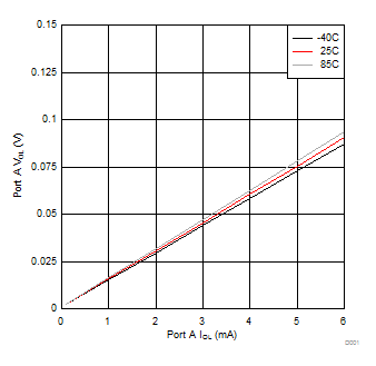
VCCA = 0.9 V, VCCB = 2.7 V Figure 1. Port A VOL vs IOL
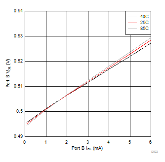
 Figure 2. Port B VOL vs IOL