JAJSC60E May 2016 – May 2021 THS6212
PRODUCTION DATA
- 1 特長
- 2 アプリケーション
- 3 概要
- 4 Revision History
- 5 Pin Configuration and Functions
- 6 Specifications
- 7 Detailed Description
- 8 Application and Implementation
- 9 Power Supply Recommendations
- 10Layout
- 11Device and Documentation Support
- 12Mechanical, Packaging, and Orderable Information
8.2.2.2.2 Computing Total Driver Power for Line-Driving Applications
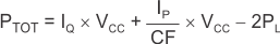
The total internal power dissipation for the THS6212 in a line-driver application is the sum of the quiescent power and the output stage power. The THS6212 holds a relatively constant quiescent current versus supply voltage—giving a power contribution that is simply the quiescent current times the supply voltage used (the supply voltage is greater than the solution given in Equation 15). The total output stage power can be computed with reference to Figure 8-8.
 Figure 8-8 Output
Stage Power Model
Figure 8-8 Output
Stage Power ModelThe two output stages used to drive the load of Figure 8-5 are shown as an H-Bridge in Figure 8-8. The average current drawn from the supply into this H-Bridge and load is the peak current in the load given by Equation 13 divided by the crest factor (CF) for the signal modulation. This total power from the supply is then reduced by the power in RT, leaving the power dissipated internal to the drivers in the four output stage transistors. That power is simply the target line power used in Equation 8 plus the power lost in the matching elements (RM). In the following examples, a perfect match is targeted giving the same power in the matching elements as in the load. The output stage power is then set by Equation 17.
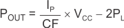
The total amplifier power is then given by Equation 18:
For the example given by Figure 8-4, the peak current is 159 mA for a signal that requires a crest factor of 5.6 with a target line power of 20.5 dBm into a 100-Ω load (115 mW).
With a typical quiescent current of 19.5 mA and a nominal supply voltage of ±14 V, the total internal power dissipation for the solution of Figure 8-4 is given by Equation 19:
