JAJSDF9D July 2017 – June 2019 TIOL111 , TIOL1113 , TIOL1115
PRODUCTION DATA.
- 1 特長
- 2 アプリケーション
- 3 概要
- 4 改訂履歴
- 5 概要(続き)
- 6 Pin Configuration and Functions
- 7 Specifications
- 8 Parameter Measurement Information
-
9 Detailed Description
- 9.1 Overview
- 9.2 Functional Block Diagrams
- 9.3
Feature Description
- 9.3.1 Wake Up Detection
- 9.3.2 Current Limit Configuration
- 9.3.3 Current Fault Detection, Indication and Auto Recovery
- 9.3.4 Thermal Warning, Thermal Shutdown
- 9.3.5 Fault Reporting (NFAULT)
- 9.3.6 Transceiver Function Tables
- 9.3.7 The Integrated Voltage Regulator (LDO)
- 9.3.8 Reverse Polarity Protection
- 9.3.9 Integrated Surge Protection and Transient Waveform Tolerance
- 9.3.10 Power Up Sequence (TIOL111)
- 9.3.11 Undervoltage Lock-Out (UVLO)
- 9.4 Device Functional Modes
- 10Application and Implementation
- 11Power Supply Recommendations
- 12Layout
- 13デバイスおよびドキュメントのサポート
- 14メカニカル、パッケージ、および注文情報
9.3.8 Reverse Polarity Protection
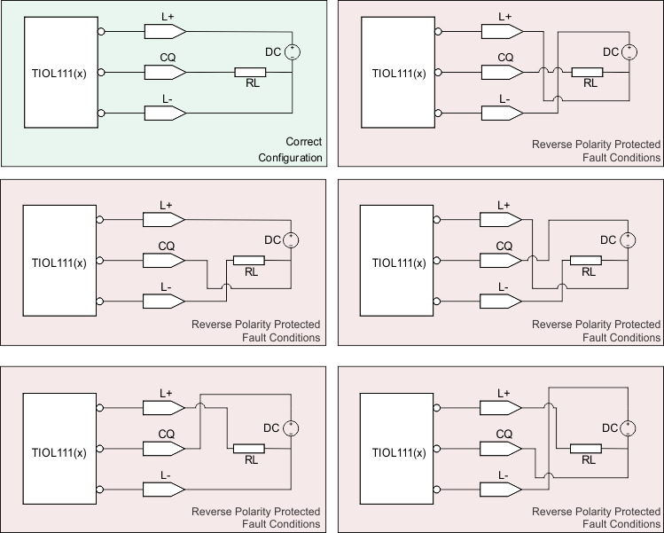
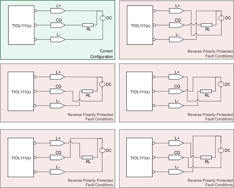
Reverse polarity protection circuitry protects the devices against accidental reverse polarity connections to the L+, CQ and L- pins. The maximum voltage between any of the pins may not exceed 60 V DC at any time.
Figure 14 and Figure 15 shows all the possible connection combinations.
 Figure 14. High-Side Driver Configuration
  Figure 15. Low-Side Driver Configuration