JAJSKP0B february 2022 – june 2023 TIOS102 , TIOS1023 , TIOS1025
PRODUCTION DATA
- 1
- 1 特長
- 2 アプリケーション
- 3 概要
- 4 Revision History
- 5 Pin Configuration and Functions
- 6 Specifications
- 7 Parameter Measurement Information
-
8 Detailed Description
- 8.1 Overview
- 8.2 Functional Block Diagrams
- 8.3
Feature Description
- 8.3.1 Current Limit Configuration
- 8.3.2 Current Fault Detection, Indication and Auto Recovery
- 8.3.3 Thermal Warning, Thermal Shutdown
- 8.3.4 Fault Reporting (NFAULT)
- 8.3.5 Device Function Tables
- 8.3.6 The Integrated Voltage Regulator (LDO)
- 8.3.7 Reverse Polarity Protection
- 8.3.8 Integrated Surge Protection and Transient Waveform Tolerance
- 8.3.9 Power Up Sequence
- 8.3.10 Undervoltage Lock-Out (UVLO)
- 8.4 Device Functional Modes
- 9 Application Information Disclaimer
- 10Power Supply Recommendations
- 11Layout
- 12Device and Documentation Support
- 13Mechanical, Packaging, and Orderable Information
パッケージ・オプション
メカニカル・データ(パッケージ|ピン)
- DRC|10
サーマルパッド・メカニカル・データ
- DRC|10
発注情報
8.3.8 Integrated Surge Protection and Transient Waveform Tolerance
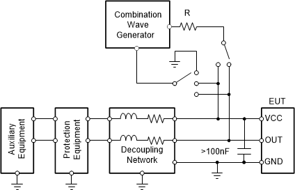
The VCC and OUT pins of the device are capable of withstanding up to 1.2 kV of 1.2/50 – 8/20 μs IEC 61000-4-5 surge with a source impedance of 500 Ω. The surge testing should be performed with a minimum 100 nF supply decoupling capacitor between VCC and GND, and 1 µF between VCC_IN/OUT and GND.
External TVS diodes may be required for higher transient protection levels. The system designer should ensure that the maximum clamping voltage of the external diodes should be < 65 V at the desired current level. The device is capable of withstanding up to ±65-V transient pulses < 100 µs.

1.2/50 - 80/20 µs CWG
R = 500 Ω
Figure 8-6 Surge Test Setup