JAJSK07C july 2012 – november 2020 TL1431-SP
PRODUCTION DATA
- 1
- 1 特長
- 2 アプリケーション
- 3 概要
- 4 Revision History
- 5 Pin Configuration and Functions
- 6 Specifications
- 7 Parameter Measurement Information
- 8 Detailed Description
- 9 Application and Implementation
- 10Power Supply Recommendations
- 11Layout
- 12Device and Documentation Support
- 13Mechanical, Packaging, and Orderable Information
パッケージ・オプション
メカニカル・データ(パッケージ|ピン)
サーマルパッド・メカニカル・データ
発注情報
6.5 Electrical Characteristics
at specified free-air temperature, IKA = 10 mA
(unless otherwise noted)
| PARAMETER | TEST CONDITIONS | TA (2) | TEST CIRCUIT | MIN | TYP | MAX | UNIT | |
|---|---|---|---|---|---|---|---|---|
| VI(ref) | Reference input voltage | VKA = VI(ref) | 25°C | Figure 7-1 | 2475 | 2500 | 2540 | mV |
| Full range | 2460 | 2550 | ||||||
| VI(dev) | Deviation of reference input voltage over full temperature range(3) | VKA = VI(ref) | Full range | Figure 7-1 | 17 | 55(1) | mV | |
 |
Ratio of change in reference input voltage to the change in cathode voltage | ΔVKA = 3 V to 36 V | Full range | Figure 7-2 | –1.1 | –2 | mV/V | |
| II(ref) | Reference input current | R1 = 10 kΩ, R2 = ∞ | 25°C | Figure 7-2 | 1.5 | 2.5 | μA | |
| Full range | 5 | |||||||
| II(dev) | Deviation of reference input current over full temperature range(3) | R1 = 10 kΩ, R2 = ∞ | Full range | Figure 7-2 | 0.5 | 3(1) | μA | |
| Imin | Minimum cathode current for regulation | VKA = VI(ref) | 25°C | Figure 7-1 | 0.45 | 1 | mA | |
| Ioff | Off-state cathode current | VKA = 36 V, VI(ref) = 0 | 25°C | Figure 7-3 | 0.18 | 0.5 | μA | |
| Full range | 2 | |||||||
| |zKA| | Output impedance(4) | VKA =
VI(ref), f ≤ 1 kHz, IKA = 1 mA to 100 mA |
25°C | Figure 7-1 | 0.2 | 0.4 | Ω | |
(1) On products compliant to MIL-PRF-38535, this parameter is not production
tested.
(2) Full range is –55°C to 125°C.
(3) The deviation parameters VI(dev) and II(dev) are
defined as the differences between the maximum and minimum values obtained over the rated
temperature range. The average full-range temperature coefficient of the reference input
voltage αVI(ref) is defined as:
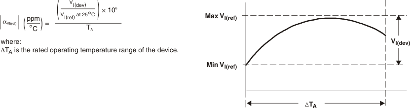
αVI(ref) is positive or negative, depending on whether minimum VI(ref) or maximum VI(ref), respectively, occurs at the lower temperature.
αVI(ref) is positive or negative, depending on whether minimum VI(ref) or maximum VI(ref), respectively, occurs at the lower temperature.
(4) The output impedance is defined as:

When the device is operating with two external resistors (see Figure 7-2), the total dynamic impedance of the circuit is given by: , which is approximately equal to
 .
.
When the device is operating with two external resistors (see Figure 7-2), the total dynamic impedance of the circuit is given by:
, which is approximately equal to
.