JAJSK07C july 2012 – november 2020 TL1431-SP
PRODUCTION DATA
- 1
- 1 特長
- 2 アプリケーション
- 3 概要
- 4 Revision History
- 5 Pin Configuration and Functions
- 6 Specifications
- 7 Parameter Measurement Information
- 8 Detailed Description
- 9 Application and Implementation
- 10Power Supply Recommendations
- 11Layout
- 12Device and Documentation Support
- 13Mechanical, Packaging, and Orderable Information
パッケージ・オプション
メカニカル・データ(パッケージ|ピン)
サーマルパッド・メカニカル・データ
発注情報
8.3 Feature Description
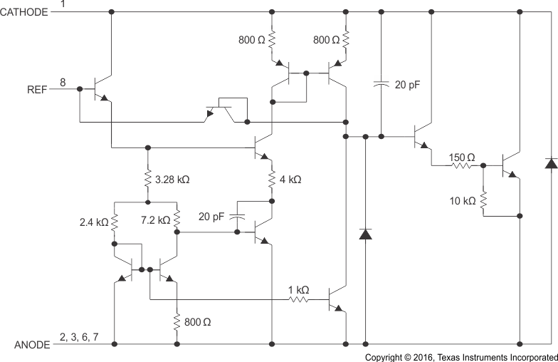
TL1431 consists of an internal reference and amplifier that outputs a sink current base on the difference between the reference pin and the virtual internal pin. The sink current is produced by the internal Darlington pair, shown in Detailed Schematic. A Darlington pair is used in order for this device to be able to sink a maximum current of 100 mA. When operated with enough voltage headroom (≥ 2.5 V) and cathode current (IKA), TL1431 forces the reference pin to 2.5 V. However, the reference pin can not be left floating, as it needs IREF ≥ 5 µA (see Electrical Characteristics – TL1431-SP). This is because the reference pin is driven into an npn, which needs base current to operate properly. When feedback is applied from the cathode and reference pins, TL1431 behaves as a Zener diode, regulating to a constant voltage dependent on current being supplied into the cathode. This is due to the internal amplifier and reference entering the proper operating regions. The same amount of current needed in the above feedback situation must be applied to this device in open loop, servo, or error amplifying implementations in order for it to be in the proper linear region giving TL1431 enough gain. Unlike many linear regulators, TL1431 is internally compensated to be stable without an output capacitor between the cathode and anode. However, if desired an output capacitor can be used as a guide to assist in choosing the correct capacitor to maintain stability.
 Figure 8-1 Symbol
 Figure 8-2 Equivalent
Schematic