JAJSHO6F March 2005 – July 2019 TL431-Q1 , TL432-Q1
PRODUCTION DATA.
- 1 特長
- 2 アプリケーション
- 3 概要
- 4 改訂履歴
- 5 Pin Configuration and Functions
- 6 Specifications
- 7 Parameter Measurement Information
- 8 Detailed Description
- 9 Application and Implementation
- 10Power Supply Recommendations
- 11Layout
- 12デバイスおよびドキュメントのサポート
- 13メカニカル、パッケージ、および注文情報
パッケージ・オプション
デバイスごとのパッケージ図は、PDF版データシートをご参照ください。
メカニカル・データ(パッケージ|ピン)
- DBZ|3
- DBV|5
サーマルパッド・メカニカル・データ
発注情報
9.2.2 Other Application Circuits
Figure 28 to Figure 40 show application circuit examples using the TL431-Q1 device. Customers must fully validate and test any circuit before implementing a design based on an example in this section. Unless otherwise noted, the design procedures in Comparator Application are applicable.
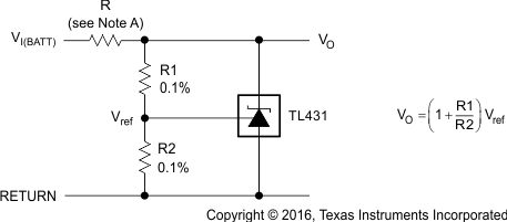
A. R must provide cathode current ≥1 mA to the TL431-Q1 at minimum VI(BATT).
Figure 28. Shunt Regulator 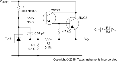
A. R must provide cathode current ≥1 mA to the TL431-Q1 at minimum VI(BATT).
Figure 30. Precision High-Current Series Regulator 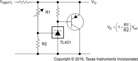 Figure 32. High-Current Shunt Regulator
 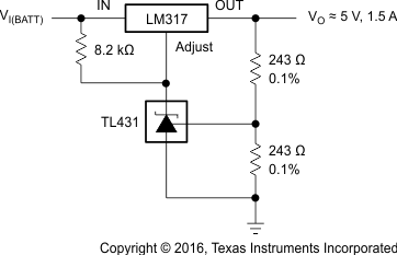 Figure 34. Precision 5-V, 1.5-A Regulator
 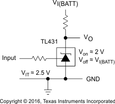 Figure 29. Single-Supply Comparator with Temperature-Compensated Threshold
 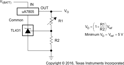 Figure 31. Output Control of a Three-Terminal Fixed Regulator
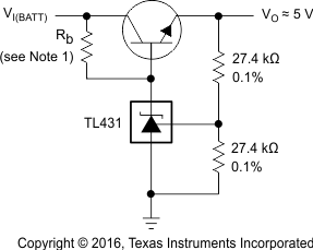
1. Rb must provide cathode current ≥1 mA to the TL431-Q1.
Figure 35. Efficient 5-V Precision Regulator 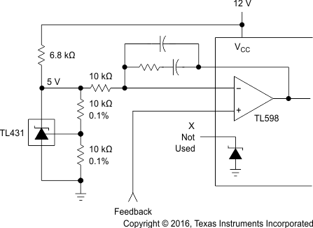 Figure 36. PWM Converter with Reference
 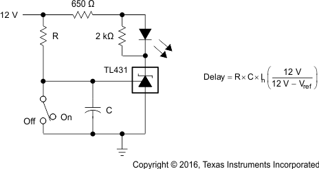 Figure 38. Delay Timer
 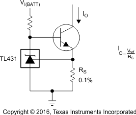 Figure 40. Precision Constant-Current Sink
A. R3 and R4 are selected to provide the desired LED intensity and cathode current ≥1 mA to the TL431-Q1 at the available VI(BATT).
Figure 37. Voltage Monitor 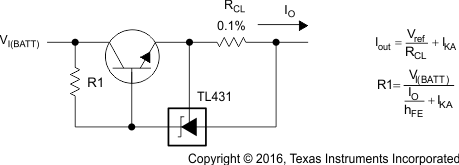 Figure 39. Precision Current Limiter