SGLS416 January 2015 TLC2274-HT
PRODUCTION DATA.
- 1 Features
- 2 Applications
- 3 Description
- 4 Revision History
- 5 Pin Configuration and Functions
-
6 Specifications
- 6.1 Absolute Maximum Ratings
- 6.2 ESD Ratings
- 6.3 Recommended Operating Conditions
- 6.4 Thermal Information
- 6.5 Electrical Characteristics, VDD = 5 V
- 6.6 Operating Characteristics, VDD = 5 V
- 6.7 Electrical Characteristics, VDD± = ±5 V
- 6.8 Operating Characteristics, VDD± = ±5 V
- 6.9 Typical Characteristics
- 7 Detailed Description
- 8 Application and Implementation
- 9 Power Supply Recommendations
- 10Layout
- 11Device and Documentation Support
- 12Mechanical, Packaging, and Orderable Information
8 Application and Implementation
NOTE
Information in the following applications sections is not part of the TI component specification, and TI does not warrant its accuracy or completeness. TI’s customers are responsible for determining suitability of components for their purposes. Customers should validate and test their design implementation to confirm system functionality.
8.1 Application Information
8.1.1 Macromodel Information
Macromodel information provided was derived using Microsim Parts, the model generation software used with Microsim PSpice. The Boyle macromodel
- Maximum positive output voltage swing
- Maximum negative output voltage swing
- Slew rate
- Quiescent power dissipation
- Input bias current
- Open-loop voltage amplification
- Unity-gain frequency
- Common-mode rejection ratio
- Phase margin
- DC output resistance
- AC output resistance
- Short-circuit output current limit
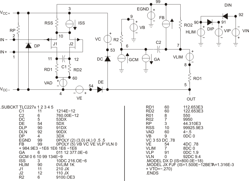 Figure 46. Boyle Macromodels and Subcircuit
8.2 Typical Application
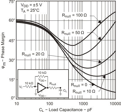
The TLC2274 is designed to drive larger capacitive loads than most CMOS operational amplifiers. Figure 48 and Figure 49 show its ability to drive loads up to 1000 pF while maintaining good gain and phase margins (Rnull = 0).
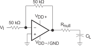 Figure 47. Typical Application Schematic
8.2.1 Design Requirements
As per Equation 1:
Table 2. Design Parameters
| Improvement in Phase Margin | UGBW (kHz) | R null (Ω) | CL (pF) |
|---|---|---|---|
| 0 | 1000 | 0 | 1000 |
| 7.15 | 1000 | 20 | 1000 |
| 17.43 | 1000 | 50 | 1000 |
| 32.12 | 1000 | 100 | 1000 |
8.2.2 Detailed Design Procedure
A smaller series resistor (Rnull) at the output of the device (see Figure 47) improves the gain and phase margins when driving large capacitive loads. Figure 48 and Figure 49 show the effects of adding series resistances of 10 Ω, 50 Ω, 100 Ω, 200 Ω, and 500 Ω. The addition of this series resistor has two effects: the first is that it adds a zero to the transfer function and the second is that it reduces the frequency of the pole associated with the output load in the transfer function.
The zero introduced to the transfer function is equal to the series resistance times the load capacitance. To calculate the improvement in phase margin, Equation 1 can be used.
where
- Δφm1 = Improvement in phase margin
- UGBW = Unity-gain bandwidth frequency
- Rnull = Output series resistance
- CL = Load capacitance
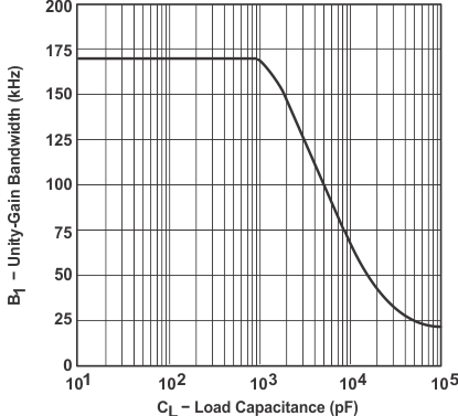
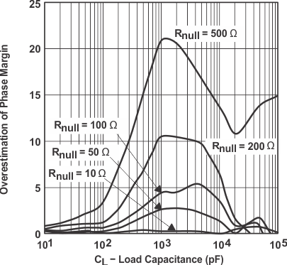
The unity-gain bandwidth (UGBW) frequency decreases as the capacitive load increases (see Figure 47). To use equation 1, UGBW must be approximated from Figure 47. Using Equation 1 alone overestimates the improvement in phase margin, as illustrated in Figure 51. The overestimation is caused by the decrease in the frequency of the pole associated with the load, thus providing additional phase shift and reducing the overall improvement in phase margin. Using Figure 47, with Equation 1 enables the designer to choose the appropriate output series resistance to optimize the design of circuits driving large capacitance loads.
8.2.3 Application Curves
TA = 25°C