SGLS416 January 2015 TLC2274-HT
PRODUCTION DATA.
- 1 Features
- 2 Applications
- 3 Description
- 4 Revision History
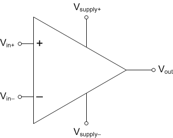
- 5 Pin Configuration and Functions
-
6 Specifications
- 6.1 Absolute Maximum Ratings
- 6.2 ESD Ratings
- 6.3 Recommended Operating Conditions
- 6.4 Thermal Information
- 6.5 Electrical Characteristics, VDD = 5 V
- 6.6 Operating Characteristics, VDD = 5 V
- 6.7 Electrical Characteristics, VDD± = ±5 V
- 6.8 Operating Characteristics, VDD± = ±5 V
- 6.9 Typical Characteristics
- 7 Detailed Description
- 8 Application and Implementation
- 9 Power Supply Recommendations
- 10Layout
- 11Device and Documentation Support
- 12Mechanical, Packaging, and Orderable Information
7 Detailed Description
7.1 Overview
The TLC2274 device exhibits rail-to-rail output performance for increased dynamic range in single- or split -supply applications. These device offers comparable ac performance while having better noise, input offset voltage and power dissipation than existing CMOS operational amplifiers. The TLC2274 device, exhibiting high input impedance and low noise, is excellent for small signal conditioning for high-impedance sources, such as piezoelectric transducers. It offers increased output dynamic range, lower noise voltage, and lower input offset voltage. This enhanced feature set allows the device to be used in a wider range of applications.
7.2 Functional Block Diagram
7.3 Feature Description
These devices use the Texas Instruments silicon gate LinCMOS™ process, giving them stable input offset voltages, very high input impedances, and extremely low input offset and bias currents. In addition, the rail-to-rail output feature with single- or split-supplies, makes this device a great choice when interfacing with analog-to-digital converters (ADCs).