SBVS237 March 2014 TLC5955
PRODUCTION DATA.
- 1 Features
- 2 Applications
- 3 Description
- 4 Revision History
- 5 Terminal Configurations and Functions
- 6 Specifications
- 7 Parameter Measurement Information
-
8 Detailed Description
- 8.1 Overview
- 8.2 Functional Block Diagram
- 8.3 Feature Description
- 8.4 Device Functional Modes
- 9 Applications and Implementation
- 10Power Supply Recommendations
- 11Layout
- 12Device and Documentation Support
- 13Mechanical, Packaging, and Orderable Information
パッケージ・オプション
メカニカル・データ(パッケージ|ピン)
サーマルパッド・メカニカル・データ
発注情報
9 Applications and Implementation
9.1 Application Information
The device is a 48-channel, constant sink current, LED driver. This device is typically connected in series to drive many LED lamps with only a few controller ports. Output current control data and PWM control data can be written from the SIN input terminal. The PWM timing reference clock can be supplied from the GSCLK input terminal. Also, the LED open and short error flag can be read out from the SOUT output terminal. Furthermore, the device maximum GSCLK clock frequency is 33 MHz and can reduce flickering discernable by the human eye.
9.2 Typical Application
9.2.1 Daisy-Chain Application
In this application, the device VCC and LED lamp anode voltages are supplied from different power supplies.
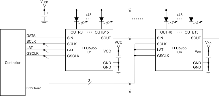 Figure 33. Multiple Daisy-Chained TLC5955 Devices
9.2.1.1 Design Requirements
For this design example, use the following as the input parameters.
Table 13. Design Parameters
| DESIGN PARAMETER | EXAMPLE VALUE |
|---|---|
| VCC input voltage range | 3.0 V to 5.5 V |
| LED lamp (VLED) input voltage range | Maximum LED forward voltage (VF) + 0.3 V (knee voltage) |
| SIN, SCLK, LAT, and GSCLK voltage range | Low level = GND, High level = VCC |
9.2.1.2 Detailed Design Procedure
9.2.1.2.1 Step-by-Step Design Procedure
To begin the design process, a few parameters must be decided upon. The designer needs to know the following:
- Maximum output constant-current value for each color LED ramp.
- Maximum LED forward voltage (VF).
- Current ratio of red, green, and blue LED lamps for the best white balance.
- Are the auto display repeat function, display timing reset function, or auto data refresh function used?
- Which PWM control method is used: ES-PWM or conventional PWM?
- Is the LED short detect (LSD) function used? If so, which detection level (70% VCC or 90% VCC) is used?
9.2.1.2.2 Maximum Current (MC) Data
There are a total of nine bits of MC data for the red, green, and blue LED ramp. Select the MC data to be greater than each LED ramp current and write the data with other control data.
9.2.1.2.3 Global Brightness Control (BC) Data
There are a total of three sets of 7-bit BC data for the red, green, and blue LED ramp. Select the BC data for the best white balance of the red, green, and blue LED ramp and write the data with other control data.
9.2.1.2.4 Dot Correction (DC) Data
There are a total of 48 sets of 7-bit DC data for each current adjustment. Select the DC data for the best uniformity of each color LED ramp and write the data with other control data.
9.2.1.2.5 Grayscale (GS) Data
There are a total of 48 sets of 16-bit GS data for the PWM control of each output. Select the GS data of the LED ramp intensity and color control and write the data with other GS data.
9.2.1.2.6 Other Control Data
There are five bits control data to set the function mode for the auto display repeat, display timing reset, auto data refresh, ES-PWM, and LSD functions explained in the Device Functional Modes section. Write the 5-bit control data for the appropriate operation of the display system with MC, BC, and DC data as the control data.
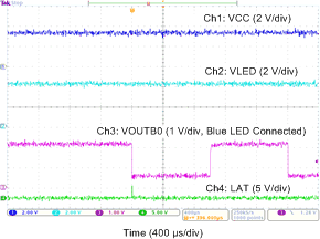
9.2.1.3 Application Curves
One LED connected to each output.
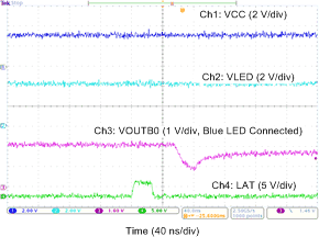
| MCX = 4 | BCX = DCXn = 7Fh | GSCLK = 33 MHz |
| VLED = 4.2 V | VCC = 3.3 V | DSPRPT = 1 |
| TMGRST, RFRESH, ESPWM, LSDVLT = 0 | ||
| MCX = 4 | BCX = DCXn = 7Fh | GSCLK = 33 MHz |
| VLED = 4.2 V | VCC = 3.3 V | DSPRPT = 1 |
| TMGRST, RFRESH, ESPWM, LSDVLT = 0 | ||