SBVS237 March 2014 TLC5955
PRODUCTION DATA.
- 1 Features
- 2 Applications
- 3 Description
- 4 Revision History
- 5 Terminal Configurations and Functions
- 6 Specifications
- 7 Parameter Measurement Information
-
8 Detailed Description
- 8.1 Overview
- 8.2 Functional Block Diagram
- 8.3 Feature Description
- 8.4 Device Functional Modes
- 9 Applications and Implementation
- 10Power Supply Recommendations
- 11Layout
- 12Device and Documentation Support
- 13Mechanical, Packaging, and Orderable Information
パッケージ・オプション
メカニカル・データ(パッケージ|ピン)
サーマルパッド・メカニカル・データ
発注情報
8 Detailed Description
8.1 Overview
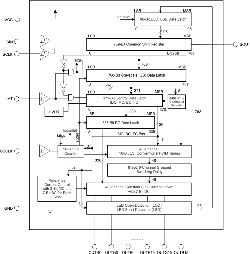
The TLC5955 is 48-channel, 30-mA, constant-current LED driver that can control LED on-time with pulse width modulation (PWM) in 65,536 steps for grayscale (GS) control. A maximum of 281 trillion colors can be generated with red, green, and blue LEDs connected to the constant-current outputs.
The device has a 128-step, 7-bit, output current control function called dot correction (DC) that can control each constant-current output. Inherently, LED lamps have different intensities resulting from manufacturing differences. The DC function can reduce the inherent differences in intensity and improve LED lamp brightness uniformity.
The device also has a 128-step, 7-bit, output current control function called global brightness control (BC) that can control each color group output. The BC function can adjust the red, green, and blue LED intensity for true white with constant-current control. The device contributes higher image quality to LED displays with fine white balance tuning by using these GS, DC, and BC functions.
The display controller can locate LED lamp failures via the device because the controller can detect LED lamp failures with the LED open detection (LOD) and LED short detection (LSD) functions and the reliability of the display can be improved by the LOD, LSD function.
The device maximum constant-current output value can be set by internal register data instead of the general method of using an external resistor setting. Thus, any failure modes that occur from the external resistor can be eliminated and one resistor can be eliminated.
The device constant-current output can drive approximately 19 mA at a 0.25-V output voltage and a +25°C ambient temperature. This voltage is called knee voltage. This 0.25-V, low-knee voltage can contribute to the design of a lower-power display system. The total number of LED drivers on one LED display panel can be reduced because 48 LED lamps can be driven by one LED driver. Therefore, designing fine-pitch LED displays is simplified.
8.2 Functional Block Diagram
8.3 Feature Description
8.3.1 Output Current Calculation
The output current value controlled by MC, DC, and BC can be calculated by Equation 1.

where:
Each output sinks the IOLCMax current when they turn on and the dot correction (DC) data and the global brightness control (BC) data are set to the maximum value of 7Fh (127d). Each output sink current can be reduced by lowering the DC and BC values.
When IOUT is set lower than 1 mA by both MC and BC or BC only, the output may be unstable. Output currents lower than 1 mA can be achieved by setting IOUT to 1 mA with MC and BC or BC only and then using DC to lower the output current.
8.3.2 Register and Data Latch Configuration
The TLC5955 has one common shift register and three data latches: the grayscale (GS) data latch, the control data latch, and the dot correction (DC) data latch. The common shift register is 769 bits long, the GS data latch is 768 bits long, the control data latch is 371 bits long, and the DC data latch is 336 bits long.
If the common shift register MSB is 0, the least significant 768 bits from the common shift register are latched into the GS data latch. If the MSB is 1, and bits 767 to 760 are 96h (10010110b), the data are latched into the control data latch. Refer to Figure 21 for the common shift register, GS data latch, control data latch, and DC data latch configurations.
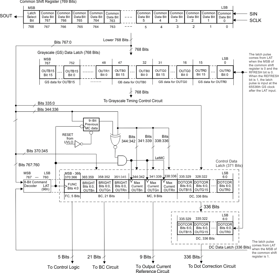 Figure 21. Common Shift Register and Data Latches Configuration
8.3.2.1 769-Bit Common Shift Register
The 769-bit common shift register is used to shift data from the SIN terminal into the TLC5955. The data shifted into the register are used for GS, DC, maximum output current, global BC functions, and function control data write operations. The common shift register LSB is connected to SIN and the MSB is connected to SOUT. On each SCLK rising edge, the data on SIN are shifted into the LSB and all 769 bits are shifted towards the MSB. The register MSB is always connected to SOUT. When the device is powered up, the data in the 769-bit common shift register are random.
8.3.2.2 Grayscale (GS) Data Latch
The GS data latch is 768 bits long, and sets the PWM timing for each constant-current output. The on-time of all constant-current outputs is controlled by the data in this data latch. The 768-bit GS data in the common shift register are copied to the data latch at a LAT rising edge when the common shift resister MSB is 0.
When the device is powered up, the data are random and all constant-current outputs are forced off. However, no outputs turn on until GS data are written to the GS data latch even if a GSCLK is input. The data bit assignment is shown in Table 1. Refer to Figure 22 for a GS data write timing diagram.
Table 1. Grayscale Data Latch Bit Description
| GS DATA LATCH BIT NUMBER | BIT NAME | DEFAULT VALUE | CONTROLLED CHANNEL | GS DATA LATCH BIT NUMBER | BIT NAME | DEFAULT VALUE | CONTROLLED CHANNEL |
|---|---|---|---|---|---|---|---|
| 15-0 | GSR0[15:0] | N/A (no default value) |
Bits[15:0] for OUTR0 | 399-384 | GSR8[15:0] | N/A (no default value) |
Bits[15:0] for OUTR8 |
| 31-16 | GSG0[15:0] | Bits[15:0] for OUTG0 | 415-400 | GSG8[15:0] | Bits[15:0] for OUTG8 | ||
| 47-32 | GSB0[15:0] | Bits[15:0] for OUTB0 | 431-416 | GSB8[15:0] | Bits[15:0] for OUTB8 | ||
| 63-48 | GSR1[15:0] | Bits[15:0] for OUTR1 | 447-432 | GSR9[15:0] | Bits[15:0] for OUTR9 | ||
| 79-64 | GSG1[15:0] | Bits[15:0] for OUTG1 | 463-448 | GSG9[15:0] | Bits[15:0] for OUTG9 | ||
| 95-80 | GSB1[15:0] | Bits[15:0] for OUTB1 | 479-464 | GSB9[15:0] | Bits[15:0] for OUTB9 | ||
| 111-96 | GSR2[15:0] | Bits[15:0] for OUTR2 | 495-480 | GSR10[15:0] | Bits[15:0] for OUTR10 | ||
| 127-112 | GSG2[15:0] | Bits[15:0] for OUTG2 | 511-496 | GSG10[15:0] | Bits[15:0] for OUTG10 | ||
| 143-128 | GSB2[15:0] | Bits[15:0] for OUTB2 | 527-512 | GSB10[15:0] | Bits[15:0] for OUTB10 | ||
| 159-144 | GSR3[15:0] | Bits[15:0] for OUTR3 | 543-528 | GSR11[15:0] | Bits[15:0] for OUTR11 | ||
| 175-160 | GSG3[15:0] | Bits[15:0] for OUTG3 | 559-544 | GSG11[15:0] | Bits[15:0] for OUTG11 | ||
| 191-176 | GSB3[15:0] | Bits[15:0] for OUTB3 | 575-560 | GSB11[15:0] | Bits[15:0] for OUTB11 | ||
| 207-192 | GSR4[15:0] | Bits[15:0] for OUTR4 | 591-576 | GSR12[15:0] | Bits[15:0] for OUTR12 | ||
| 223-208 | GSG4[15:0] | Bits[15:0] for OUTG4 | 607-592 | GSG12[15:0] | Bits[15:0] for OUTG12 | ||
| 239-224 | GSB4[15:0] | Bits[15:0] for OUTB4 | 623-608 | GSB12[15:0] | Bits[15:0] for OUTB12 | ||
| 255-240 | GSR5[15:0] | Bits[15:0] for OUTR5 | 639-624 | GSR13[15:0] | Bits[15:0] for OUTR13 | ||
| 271-256 | GSG5[15:0] | Bits[15:0] for OUTG5 | 655-640 | GSG13[15:0] | Bits[15:0] for OUTG13 | ||
| 287-272 | GSB5[15:0] | Bits[15:0] for OUTB5 | 671-656 | GSB13[15:0] | Bits[15:0] for OUTB13 | ||
| 303-288 | GSR6[15:0] | Bits[15:0] for OUTR6 | 687-672 | GSR14[15:0] | Bits[15:0] for OUTR14 | ||
| 319-304 | GSG6[15:0] | Bits[15:0] for OUTG6 | 703-688 | GSG14[15:0] | Bits[15:0] for OUTG14 | ||
| 335-320 | GSB6[15:0] | Bits[15:0] for OUTB6 | 719-704 | GSB14[15:0] | Bits[15:0] for OUTB14 | ||
| 351-336 | GSR7[15:0] | Bits[15:0] for OUTR7 | 735-720 | GSR15[15:0] | Bits[15:0] for OUTR15 | ||
| 367-352 | GSG7[15:0] | Bits[15:0] for OUTG7 | 751-736 | GSG15[15:0] | Bits[15:0] for OUTG15 | ||
| 383-368 | GSB7[15:0] | Bits[15:0] for OUTB7 | 767-752 | GSB15[15:0] | Bits[15:0] for OUTB15 |
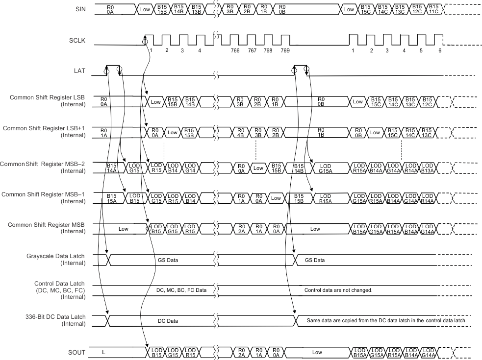 Figure 22. Grayscale Data Write Timing Diagram (RFRESH = 0)
8.3.2.3 Control Data Latch
The control data latch is 371 bits long. The data latch contains dot correction (DC) data, maximum current (MC) data, global brightness control (BC) data, and function control (FC) data. The DC for each constant-current output are controlled by the data in the DC data latch. The control data in the data latch are updated with the lower 371 bits of the common shift register at the LAT rising edge when the common shift register MSB is 1. The 336 bits of DC data are copied from the control data latch when the 65,536th GSCLK is input with RFRESH set to 1 in the control data latch after the GS data are written or the LAT rising edge for GS data writes is input when the RFRESH bit is 0.
When the device is powered up, the data in the control data latch (except the MC bits) are random. Therefore, DC, BC, and FC data must be written to the control data latch before turning on the constant-current outputs. Furthermore, MC data should be set appropriately for the application. Refer to Figure 23 for a control data write timing diagram.
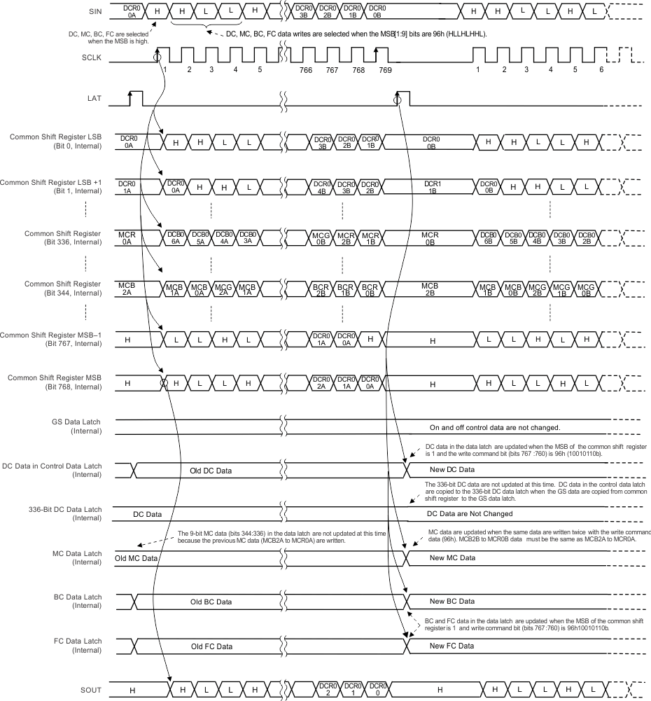 Figure 23. Control Data Write Timing Diagram for DC, MC, BC, and FC
8.3.2.4 Dot Correction (DC) Data Latch
DC data are 336 bits long; the data for each constant-current output are controlled by seven bits. Each constant-current output DC is controlled by the DC data latch. Each DC value individually adjusts the output current for each constant-current output. As explained in the Dot Correction (DC) Function section, the DC values are used to adjust the output current from 26.2% to 100% of the current value set by MC and BC data. When the device is powered on, the data in the DC data latch are random.
The DC data bit assignment is shown in Table 2. See Table 9 for a summary of the DC data value versus set current value.
Table 2. Dot Correction Data Bit Description
| CONTROL DATA LATCH BIT NUMBER | BIT NAME | DEFAULT VALUE | CONTROLLED CHANNEL | CONTROL DATA LATCH BIT NUMBER | BIT NAME | DEFAULT VALUE | CONTROLLED CHANNEL |
|---|---|---|---|---|---|---|---|
| 6-0 | DCR0[6:0] | N/A (no default value) |
DC bits[6:0] for OUTR0 | 174-168 | DCR8[6:0] | N/A (no default value) |
DC bits[6:0] for OUTR8 |
| 13-7 | DCG0[6:0] | DC bits[6:0] for OUTG0 | 181-175 | DCG8[6:0] | DC bits[6:0] for OUTG8 | ||
| 20-14 | DCB0[6:0] | DC bits[6:0] for OUTB0 | 188-182 | DCB8[6:0] | DC bits[6:0] for OUTB8 | ||
| 27-21 | DCR1[6:0] | DC bits[6:0] for OUTR1 | 195-189 | DCR9[6:0] | DC bits[6:0] for OUTR9 | ||
| 34-28 | DCG1[6:0] | DC bits[6:0] for OUTG1 | 202-196 | DCG9[6:0] | DC bits[6:0] for OUTG9 | ||
| 41-35 | DCB1[6:0] | DC bits[6:0] for OUTB1 | 209-203 | DCB9[6:0] | DC bits[6:0] for OUTB9 | ||
| 48-42 | DCR2[6:0] | DC bits[6:0] for OUTR2 | 216-210 | DCR10[6:0] | DC bits[6:0] for OUTR10 | ||
| 55-49 | DCG2[6:0] | DC bits[6:0] for OUTG2 | 223-217 | DCG10[6:0] | DC bits[6:0] for OUTG10 | ||
| 62-56 | DCB2[6:0] | DC bits[6:0] for OUTB2 | 230-224 | DCB10[6:0] | DC bits[6:0] for OUTB10 | ||
| 69-63 | DCR3[6:0] | DC bits[6:0] for OUTR3 | 237-231 | DCR11[6:0] | DC bits[6:0] for OUTR11 | ||
| 76-70 | DCG3[6:0] | DC bits[6:0] for OUTG3 | 244-238 | DCG11[6:0] | DC bits[6:0] for OUTG11 | ||
| 83-77 | DCB3[6:0] | DC bits[6:0] for OUTB3 | 251-245 | DCB11[6:0] | DC bits[6:0] for OUTB11 | ||
| 90-84 | DCR4[6:0] | DC bits[6:0] for OUTR4 | 258-252 | DCR12[6:0] | DC bits[6:0] for OUTR12 | ||
| 97-91 | DCG4[6:0] | DC bits[6:0] for OUTG4 | 265-259 | DCG12[6:0] | DC bits[6:0] for OUTG12 | ||
| 104-98 | DCB4[6:0] | DC bits[6:0] for OUTB4 | 272-266 | DCB12[6:0] | DC bits[6:0] for OUTB12 | ||
| 111-105 | DCR5[6:0] | DC bits[6:0] for OUTR5 | 279-273 | DCR13[6:0] | DC bits[6:0] for OUTR13 | ||
| 118-112 | DCG5[6:0] | DC bits[6:0] for OUTG5 | 286-280 | DCG13[6:0] | DC bits[6:0] for OUTG13 | ||
| 125-119 | DCB5[6:0] | DC bits[6:0] for OUTB5 | 293-287 | DCB13[6:0] | DC bits[6:0] for OUTB13 | ||
| 132-126 | DCR6[6:0] | DC bits[6:0] for OUTR6 | 300-294 | DCR14[6:0] | DC bits[6:0] for OUTR14 | ||
| 139-133 | DCG6[6:0] | DC bits[6:0] for OUTG6 | 307-301 | DCG14[6:0] | DC bits[6:0] for OUTG14 | ||
| 146-140 | DCB6[6:0] | DC bits[6:0] for OUTB6 | 314-308 | DCB14[6:0] | DC bits[6:0] for OUTB14 | ||
| 153-147 | DCR7[6:0] | DC bits[6:0] for OUTR7 | 321-315 | DCR15[6:0] | DC bits[6:0] for OUTR15 | ||
| 160-154 | DCG7[6:0] | DC bits[6:0] for OUTG7 | 328-322 | DCG15[6:0] | DC bits[6:0] for OUTG15 | ||
| 167-161 | DCB7[6:0] | DC bits[6:0] for OUTB7 | 335-329 | DCB15[6:0] | DC bits[6:0] for OUTB15 |
8.3.2.5 Maximum Current (MC) Data Latch
The maximum output current per channel, IOLCMax, is programmed by MC data and can be set with the serial interface. IOLCMax is the largest current for each output. Each output sinks the IOLCMax current when they turn on with DC and BC data set to the maximum value of 7Fh (127d). MC data must have the same data continuously written twice in order to change the data. When the device is powered on, the MC data are set to 0.
The MC data bit assignment is shown in Table 3. See Table 8 for a summary of the MC data value for each color group versus the set current value.
Table 3. Maximum Current Data Bit Assignment in the Control Data Latch
| CONTROL DATA LATCH BIT NUMBER | BIT NAME | DEFAULT VALUE | CONTROLLED CHANNEL |
|---|---|---|---|
| 338-336 | MCR[2:0] | 0 | MC bits[2:0] for red color group channels (OUTR0 to OUTR15) |
| 341-339 | MCG[2:0] | 0 | MC bits[2:0] for green color group channels (OUTG0 to OUTG15) |
| 344-342 | MCB[2:0] | 0 | MC bits[2:0] for blue color group channels (OUTB0 to OUTB15) |
8.3.2.6 Global Brightness Control (BC) Data Latch
Global BC data are seven bits long. The global brightness for all outputs is controlled by the data in the control data latch. The data are used to adjust the constant-current values for the 48-channel constant-current outputs. As explained in the Global Brightness Control (BC) Function section, the BC values are used to adjust the output current from 10% to 100% of the maximum value. When the device is powered on, the BC data are random.
The global BC data bit assignment in the control data latch is shown in Table 4. See Table 10 for a summary of the BC data value versus set current value.
Table 4. Global Brightness Control Data Bit Assignment in the Control Data Latch
| CONTROL DATA LATCH BIT NUMBER | BIT NAME | DEFAULT VALUE | CONTROLLED CHANNEL |
|---|---|---|---|
| 351-345 | BCR[6:0] | N/A (no default value) | BC bits[6:0] for red color group channels (OUTR0 to OUTR15) |
| 358-352 | BCG[6:0] | BC bits[6:0] for green color group channels (OUTG0 to OUTG15) | |
| 365-359 | BCB[6:0] | BC bits[6:0] for blue color group channels (OUTB0 to OUTB15) |
8.3.2.7 Function Control (FC) Data Latch
The FC data latch is 5 bits long. This latch enables the auto display repeat and display timing reset functions, and sets the DC data auto refresh, PWM control mode, and the LSD detection voltage. Each function is selected by the data in the control data latch. When the device is powered on, the FC data are random. The FC data bit assignment in the control data latch is shown in Table 5.
Table 5. Function Control Data Latch Bit Description
| BIT NUMBER |
BIT NAME |
DEFAULT VALUE (Binary) |
DESCRIPTION |
|---|---|---|---|
| 366 | DSPRPT | N/A (no default value) |
Auto display repeat mode enable bit 0 = Disabled, 1 = Enabled When this bit is 0, the auto display repeat function is disabled. Each constant-current output is turned on and off for one display period. When this bit is 1, each output repeats the PWM control every 65,536 GSCLKs. |
| 367 | TMGRST | Display timing reset mode enable bit 0 = Disabled, 1 = Enabled When this bit is 0, the GS counter is not reset and the outputs are not forced off even when a LAT rising edge is input for a GS data write. When this bit is 1, the GS counter is reset to 0 and all outputs are forced off at the LAT rising edge for a GS data write. Afterwards, PWM control resumes from the next GSCLK rising edge. |
|
| 368 | RFRESH | Auto data refresh mode enable bit 0 = Disabled, 1 = Enabled When this bit is 0, the auto data refresh function is disabled. The data in the common shift register are copied to the GS data latch at the next LAT rising edge for a GS data write. DC data in the control data latch are copied to the DC data latch at the same time. When this bit is 1, the auto data refresh function is enabled. The data in the common shift register are copied to the GS data latch at the 65,536th GSCLK after the LAT rising edge for a GS data write. DC data in the control data latch are copied to the DC data latch at the same time. |
|
| 369 | ESPWM | ES-PWM mode enable bit 0 = Disabled, 1 = Enabled When this bit is 0, the conventional PWM control mode is selected. If the TLC5955 is used for multiplexing a drive, the conventional PWM mode should be selected to prevent excess on or off switching. When this bit is 1, ES-PWM control mode is selected. |
|
| 370 | LSDVLT | LSD detection voltage selection bit LED short detection (LSD) detects a fault caused by a shorted LED by comparing the OUTXn voltage to the LSD detection threshold voltage. The threshold voltage is selected by this bit. When this bit is 0, the LSD voltage is VCC × 70%. When this bit is 1, the LSD voltage is VCC × 90%. |
8.3.3 Status Information Data (SID)
The status information data (SID) contains the status of the LED open detection (LOD) and LED short detection (LSD). When the MSB of the common shift register is set to 0 and the RFRESH bit in the control data latch is 0, the SID are loaded to the common shift register at the LAT falling edge after the data in the common shift register are loaded to the grayscale data latch. If the common shift register MSB is 1, the SID are not loaded to the common shift register.
When the MSB of the common shift register is set to 0 and the RFRESH bit in the control data latch is 1, the SID are loaded to the common shift register at the GS counter 0000h just after LAT when the GS data are input. If the common shift register MSB is 1, the SID are not loaded to the common shift register. When the RFRESH bit is 1, the SCLK rising edge must be input with a low-level LAT signal after 65,538 GSCLKs (or more) are input from the LAT rising signal input.
After being loaded into the common shift register, new SID data cannot be loaded until at least one new bit of data is written into the common shift register. To recheck SID without changing the GS data, reprogram the common shift register with the same data currently programmed into the GS latch. When LAT goes high, the GS data do not change, but new SID data are loaded into the common shift register. LOD and LSD are shifted out of SOUT with each SCLK rising edge. The SID load configuration is shown in Figure 24 and Table 6.
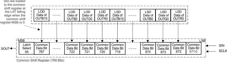 Figure 24. SID Load Configuration
Table 6. SID Load Description
| COMMON SHIFT REGISTER BIT NUMBER | LOADED SID | COMMON SHIFT REGISTER BIT NUMBER | LOADED SID |
|---|---|---|---|
| 671-0 | No data loaded | 720 | OUTR0 LOD data |
| 672 | OUTR0 LSD data (0 = No error, 1 = Error) |
721 | OUTG0 LOD data |
| 673 | OUTG0 LSD data | 722 | OUTB0 LOD data |
| 674 | OUTB0 LSD data | 723 | OUTR1 LOD data |
| 675 | OUTR1 LSD data | 724 | OUTG1 LOD data |
| 676 | OUTG1 LSD data | 725 | OUTB1 LOD data |
| 677 | OUTB1 LSD data | 726 | OUTR2 LOD data |
| 678 | OUTR2 LSD data | 727 | OUTG2 LOD data |
| 679 | OUTG2 LSD data | 728 | OUTB2 LOD data |
| 680 | OUTB2 LSD data | 729 | OUTR3 LOD data |
| 681 | OUTR3 LSD data | 730 | OUTG3 LOD data |
| 682 | OUTG3 LSD data | 731 | OUTB3 LOD data |
| 683 | OUTB3 LSD data | 732 | OUTR4 LOD data |
| 684 | OUTR4 LSD data | 733 | OUTG4 LOD data |
| 685 | OUTG4 LSD data | 734 | OUTB4 LOD data |
| 686 | OUTB4 LSD data | 735 | OUTR5 LOD data |
| 687 | OUTR5 LSD data | 736 | OUTG5 LOD data |
| 688 | OUTG5 LSD data | 737 | OUTB5 LOD data |
| 689 | OUTB5 LSD data | 738 | OUTR6 LOD data |
| 690 | OUTR6 LSD data | 739 | OUTG6 LOD data |
| 691 | OUTG6 LSD data | 740 | OUTB6 LOD data |
| 692 | OUTB6 LSD data | 741 | OUTR7 LOD data |
| 693 | OUTR7 LSD data | 742 | OUTG7 LOD data |
| 694 | OUTG7 LSD data | 743 | OUTB7 LOD data |
| 695 | OUTB7 LSD data | 744 | OUTR8 LOD data |
| 696 | OUTR8 LSD data | 745 | OUTG8 LOD data |
| 697 | OUTG8 LSD data | 746 | OUTB8 LOD data |
| 698 | OUTB8 LSD data | 747 | OUTR9 LOD data |
| 699 | OUTR9 LSD data | 748 | OUTG9 LOD data |
| 700 | OUTG9 LSD data | 749 | OUTB9 LOD data |
| 701 | OUTB9 LSD data | 750 | OUTR10 LOD data |
| 702 | OUTR10 LSD data | 751 | OUTG10 LOD data |
| 703 | OUTG10 LSD data | 752 | OUTB10 LOD data |
| 704 | OUTB10 LSD data | 753 | OUTR11 LOD data |
| 705 | OUTR11 LSD data | 754 | OUTG11 LOD data |
| 706 | OUTG11 LSD data | 755 | OUTB11 LOD data |
| 707 | OUTB11 LSD data | 756 | OUTR12 LOD data |
| 708 | OUTR12 LSD data | 757 | OUTG12 LOD data |
| 709 | OUTG12 LSD data | 758 | OUTB12 LOD data |
| 710 | OUTB12 LSD data | 759 | OUTR13 LOD data |
| 711 | OUTR13 LSD data | 760 | OUTG13 LOD data |
| 712 | OUTG13 LSD data | 761 | OUTB13 LOD data |
| 713 | OUTB13 LSD data | 762 | OUTR14 LOD data |
| 714 | OUTR14 LSD data | 763 | OUTG14 LOD data |
| 715 | OUTG14 LSD data | 764 | OUTB14 LOD data |
| 716 | OUTB14 LSD data | 765 | OUTR15 LOD data |
| 717 | OUTR15 LSD data | 766 | OUTG15 LOD data |
| 718 | OUTG15 LSD data | 767 | OUTB15 LOD data |
| 719 | OUTB15 LSD data | 768 | No data loaded |
8.3.4 LED Open Detection (LOD)
LOD detects a fault caused by an LED open circuit or a short from OUTXn to ground with low resistance by comparing the OUTXn voltage to the LOD detection threshold voltage (0.3 V, typically). If the OUTXn voltage is lower than the threshold voltage when OUTXn is on, that output LOD bit is set to 1 to indicate an open LED. Otherwise, the LOD bit is set to 0. LOD data are only valid for outputs that are programmed to be on. LOD data are latched into the LOD, LSD data latch at the 33rd GSCLK. LOD data for outputs programmed to be off at the 33rd GSCLK are always 0. The LED open detection circuit is shown in Figure 25 and Table 7 lists an LOD truth table. Refer to Figure 26 for an LOD read timing diagram.
8.3.5 LED Short Detection (LSD)
LSD data detect a fault caused by a shorted LED between LED terminals by comparing the OUTXn voltage to the LSD detection threshold voltage level set by LSDVLT in the control data latch. If the OUTXn voltage is higher than the programmed voltage when OUTXn is on, the corresponding output LSD bit is set to 1 to indicate a shorted LED. Otherwise, the LSD bit is set to 0. LSD data are only valid for outputs that are programmed to be on. LSD data are latched into the LOD, LSD data latch at the 33rd GSCLK. LSD data for outputs programmed to be off at the 33rd GSCLK are always 0. The LSD open detection circuit is shown in Figure 25 and Table 7 lists an LSD truth table. Refer to Figure 26 for an LSD read timing diagram.
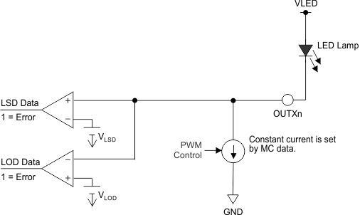 Figure 25. LOD and LSD Circuit
Table 7. LOD and LSD Truth Table
| SID DATA | CONDITION | |
|---|---|---|
| LOD | LSD | |
| 0 | LED is not opened (VOUTXn > VLOD) | LED is not shorted (VOUTXn ≤ VLSD) |
| 1 | LED is open or shorted to GND (VOUTXn ≤ VLOD) | LED is shorted between anode and cathode, or shorted to higher voltage side (VOUTXn > VLSD) |
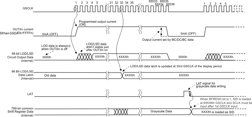 Figure 26. LOD and LSD Read and Load Timing Diagram
8.3.6 Noise Reduction
Large surge currents may flow through the device and the board on which the device is mounted if all 48 outputs turn on simultaneously at the start of each GS cycle. These large current surges can introduce detrimental noise and electromagnetic interference (EMI) into other circuits. The TLC5955 independently turns the outputs on with a series delay for each group to provide a soft-start feature. The output current sinks are grouped into eight groups. The first output group that is turned on or off are OUTR4, OUTG4, OUTB4, OUTR11, OUTG11, and OUTB11; the second output group is OUTX0 and OUTX15; the third output group is OUTX5 and OUTX10; the fourth output group is OUTX1 and OUTX14; the fifth output group is OUTX2 and OUTX13; the sixth output group is OUTX6 and OUTX9; the seventh output group is OUTX3 and OUTX12; and the eighth output group is OUTX7 and OUTX8. Each output group is turned on and off sequentially with a small delay between groups.
8.4 Device Functional Modes
8.4.1 Maximum Current Control (MC) Function
The maximum output current per channel, IOLCMax, is programmed by the MC data and is set with the serial interface. IOLCMax is the largest current for each output. Each OUTXn sinks the IOLCMax current when they turn on and the dot correction and global brightness control data are set to the maximum value of 7Fh (127d).
When the device is powered on, the MC data are set to 0. MC data should be changed when all constant-current outputs (OUTXn, where X = R, G, or B; n = 0 to 7) are off. MCX = 6 and MCX = 7 are used when VCC is greater than 3.6 V. The same MC data must be written twice to change the maximum constant-current output. Table 8 shows the characteristics of the constant-current sink versus the maximum current (MC) control data.
Table 8. Maximum Constant-Current Output versus MC Data
| MCX(2) DATA | IOLCMax (mA), OUTXn(3) | ||
|---|---|---|---|
| BINARY | DECIMAL | HEX | |
| 000 (default) | 0 (default) | 0 (default) | 3.2 |
| 001 | 1 | 1 | 8.0 |
| 010 | 2 | 2 | 11.2 |
| 011 | 3 | 3 | 15.9 |
| 100 | 4 | 4 | 19.1 |
| 101 | 5 | 5 | 23.9 |
| 110(1) | 6 | 6 | 27.1 |
| 111(1) | 7 | 7 | 31.9 |
8.4.2 Dot Correction (DC) Function
The TLC5955 can individually adjust the output current of each channel (OUTx0 to OUTx15, where x is R, G, or B) by using DC. The DC function allows the brightness deviations of the LEDs connected to each output to be individually adjusted. Each output DC is programmed with a 7-bit word, so the value is adjusted with 128 steps within the range of 26.2% to 100% of IOLCMax. DC data are programmed into the TLC5955 with the serial interface. When the device is powered on, the DC data in the control latch contains random data. Therefore, DC data must be written to the DC data latch before turning the constant-current outputs on. Table 9 summarizes the DC data value versus the set current value.
Table 9. DC Data versus Current Ratio and Set Current Value
| DCXn(3) DATA | BC DATA (Hex) | RATIO OF OUTPUT CURRENT TO IOLCMax (%) | IOUT (mA) (MC = 7, typical) |
IOUT (mA) (MC = 0, typical) |
||
|---|---|---|---|---|---|---|
| BINARY | DECIMAL | HEX | ||||
| 000 0000 | 0 | 00 | 7F | 26.2 | 8.36 | 0.84 |
| 000 0001 | 1 | 01 | 7F | 26.7 | 8.54 | 0.86 |
| 000 0010 | 2 | 02 | 7F | 27.3 | 8.73 | 0.88 |
| — | — | — | — | — | — | — |
| 111 1101 | 125 | 7D | 7F | 98.8 | 31.5 | 3.16 |
| 111 1110 | 126 | 7E | 7F | 99.4 | 31.7 | 3.18 |
| 111 1111 | 127 | 7F | 7F | 100.0 | 31.9 | 3.20 |
8.4.3 Global Brightness Control (BC) Function
The TLC5955 has the ability to adjust the output current of all constant-current outputs of each color group (OUTR0 to OUTR15, OUTG0 to OUTG15, and OUTB0 to OUTB15) simultaneously to the same current ratio. This function is called global brightness control (BC). The BC function allows the global brightness of LEDs connected to the output to be adjusted. All outputs of each color group can be adjusted in 128 steps from 10% to 100% of the maximum output current, IOLCMax. BC data are programmed into the TLC5955 with the serial interface. When the BC data change, the output current also changes immediately. When the device is powered on, the BC data contain random data. Table 10 summarizes the BC data versus the set current value.
Table 10. BC Data versus Constant-Current Ratio and Set Current Value
| BCX(2) DATA | DCXn(3) DATA (Hex) | RATIO OF OUTPUT CURRENT TO IOLCMax(%) | IOUT (mA) (MC = 7, typical) |
IOUT (mA) (MC = 0, typical) |
||
|---|---|---|---|---|---|---|
| BINARY | DECIMAL | HEX | ||||
| 000 0000 | 0 | 00 | 7F | 10.0 | 3.19 | 0.32 |
| 000 0001 | 1 | 01 | 7F | 10.7 | 3.42 | 0.34 |
| 000 0010 | 2 | 02 | 7F | 11.4 | 3.64 | 0.37 |
| — | — | — | — | — | — | — |
| 111 1101 | 125 | 7D | 7F | 98.6 | 31.5 | 3.15 |
| 111 1110 | 126 | 7E | 7F | 99.3 | 31.7 | 3.18 |
| 111 1111 | 127 | 7F | 7F | 100.0 | 31.9 | 3.20 |
8.4.4 Grayscale (GS) Function (PWM Control)
The TLC5955 can adjust the brightness of each output channel using a pulse width modulation (PWM) control scheme. The architecture of 16 bits per channel results in 65,536 brightness steps, from 0% up to 100% brightness.
The PWM operation for OUTn is controlled by a 16-bit grayscale (GS) counter. The GS counter increments on each GS reference clock (GSCLK) rising edge. The GS counter resets to 0000h when the LAT rising signal for a GS data write is input with the display timing reset mode enabled.
The TLC5955 has two types of PWM control: conventional PWM control and enhanced spectrum (ES) PWM control. The conventional PWM control can be selected when the ESPWM bit in the control data latch is 0. The ES PWM control is selected when the ESPWM bit is 1. The conventional PWM control should be selected for multiplexing a drive. The ES-PWM control should be selected for a static drive.
The on-time (tOUT_ON) of each output (OUTn) can be calculated by Equation 2.
where:
Table 11 summarizes the GS data values versus the output on-time duty cycle. When the device powers up, all OUTXn are forced off, the GS counter initializes to 0000h, and the status remains the same until GS data are written. After that, each OUTXn on and off status can be controlled by GS data and GSCLK.
Table 11. Output Duty Cycle and On-Time versus GS Data
| GS DATA | ON-TIME DUTY (%) | GS DATA | ON-TIME DUTY (%) | ||
|---|---|---|---|---|---|
| DECIMAL | HEX | DECIMAL | HEX | ||
| 0 | 0 | 0 | 32768 | 8000 | 50.000 |
| 1 | 1 | 0.002 | 32769 | 8001 | 50.002 |
| 2 | 2 | 0.003 | 32770 | 8002 | 50.003 |
| 3 | 3 | 0.005 | 32771 | 8003 | 50.005 |
| — | — | — | — | — | — |
| 8191 | 1FFF | 12.498 | 40959 | 9FFF | 62.498 |
| 8192 | 2000 | 12.500 | 40960 | A000 | 62.500 |
| 8193 | 2001 | 12.502 | 40961 | A001 | 62.502 |
| — | — | — | — | — | — |
| 16381 | 3FFD | 24.996 | 49149 | BFFD | 74.995 |
| 16382 | 3FFE | 24.997 | 49150 | BFFE | 74.997 |
| 16383 | 3FFF | 24.998 | 49151 | BFFF | 74.998 |
| 16384 | 4000 | 25.000 | 49152 | C000 | 75.000 |
| 16385 | 4001 | 25.002 | 49153 | C001 | 75.002 |
| 16386 | 4002 | 25.003 | 49154 | C002 | 75.003 |
| 16387 | 4003 | 25.005 | 49155 | C003 | 75.005 |
| — | — | — | — | — | — |
| 24575 | 5FFF | 37.498 | 57343 | DFFF | 87.498 |
| 24576 | 6000 | 37.500 | 57344 | E000 | 87.500 |
| 24577 | 6001 | 37.502 | 57345 | E001 | 87.502 |
| — | — | — | — | — | — |
| 32765 | 7FFD | 49.995 | 65533 | FFFD | 99.995 |
| 32766 | 7FFE | 49.997 | 65534 | FFFE | 99.997 |
| 32767 | 7FFF | 49.998 | 65535 | FFFF | 99.998 |
8.4.4.1 Conventional PWM Control
The first GS clock rising edge increments the GS counter by one and switches on all outputs with a non-zero GS value programmed into the GS data latch. Each additional GS clock rising edge increases the corresponding GS counter by one.
The GS counter keeps track of the number of clock pulses from the respective GS clock inputs. Each output stays on while the counter is less than or equal to the programmed GS value. Each output turns off at the GS counter value rising edge when the counter becomes greater than the output GS latch value. Figure 27 illustrates the conventional PWM operation.
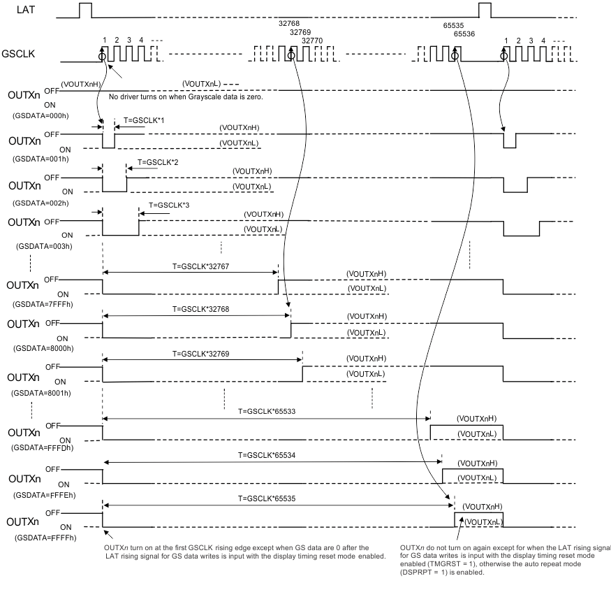 Figure 27. Conventional PWM Operation
8.4.4.2 Enhanced Spectrum (ES) PWM Control
In this PWM control, the total display period is divided into 128 display segments. The total display period is the time from the first GS clock (GSCLK) to the 65,536th GSCLK input. Each display segment has a maximum of 512 GSCLKs. The OUTXn on-time changes, depending on the 16-bit GS data. Refer to Table 12 for the sequence of information and to Figure 28 for the timing information.
Table 12. ES PWM Drive Turn On-Time Length
| GS DATA | OUTn DRIVER OPERATION | |
|---|---|---|
| DECIMAL | HEX | |
| 0 | 0000h | Does not turn on |
| 1 | 0001h | Turns on for one GSCLK period in the first display segment |
| 2 | 0002h | Turns on for one GSCLK period in the first and 65th display segments |
| 3 | 0003h | Turns on for one GSCLK period in the first, 65th, and 33rd display segments |
| 4 | 0004h | Turns on for one GSCLK period in the first, 65th, 33rd, and 97th display segments |
| 5 | 0005h | Turns on for one GSCLK period in the first, 65th, 33rd, 97th, and 17th display segments |
| 6 | 0006h | Turns on for one GSCLK period in the first, 65th, 33rd, 97th, 17th, and 81st display segments |
| — | — | The number of display segments where OUTn is turned on for one GSCLK is incremented by increasing GS data in the following order: 1 > 65 > 33 > 97 > 17 > 81 > 49 > 113 > 9 > 73 > 41 > 105 > 25 > 89 > 57 > 121 > 5 > 69 > 37 > 101 > 21 > 85 > 53 > 117 > 13 > 77 > 45 > 109 > 29 > 93 > 61 > 125 > 3 > 67 > 35 > 99 > 19 > 83 > 51 > 115 > 11 > 75 > 43 > 107 > 27 > 91 > 59 > 123 > 7 > 71 > 39 > 103 > 23 > 87 > 55 > 119 > 15 > 79 > 47 > 111 > 31 > 95 > 63 > 127 > 2 > 66 > 34 > 98 > 18 > 82 > 50 > 114 > 10 > 74 > 42 > 106 > 26 > 90 > 58 > 122 > 6 > 70 > 38 > 102 > 22 > 86 > 54 > 118 > 14 > 78 > 46 > 110 > 30 > 94 > 62 > 126 > 4 > 68 > 36 > 100 > 20 > 84 > 52 > 116 > 12 > 76 > 44 > 108 > 28 > 92 > 60 > 124 > 8 > 72 > 40 > 104 > 24 > 88 > 56 > 120 > 16 > 80 > 48 > 112 > 32 > 96 > 64 > 128. |
| 127 | 007Fh | Turns on for one GSCLK period in the first to 127th display segments, but does not turn on in the 128th display segment |
| 128 | 0080h | Turns on for one GSCLK period in all display segments (first to 128th) |
| 129 | 0081h | Turns on for two GSCLK periods in the first display period and for one GSCLK period in all other display periods |
| — | — | The number of display segments where OUTn is turned on for one GSCLK is incremented by increasing GS data in the following order: 1 > 65 > 33 > 97 > 17 > 81 > 49 > 113 > 9 > 73 > 41 > 105 > 25 > 89 > 57 > 121 > 5 > 69 > 37 > 101 > 21 > 85 > 53 > 117 > 13 > 77 > 45 > 109 > 29 > 93 > 61 > 125 > 3 > 67 > 35 > 99 > 19 > 83 > 51 > 115 > 11 > 75 > 43 > 107 > 27 > 91 > 59 > 123 > 7 > 71 > 39 > 103 > 23 > 87 > 55 > 119 > 15 > 79 > 47 > 111 > 31 > 95 > 63 > 127 > 2 > 66 > 34 > 98 > 18 > 82 > 50 > 114 > 10 > 74 > 42 > 106 > 26 > 90 > 58 > 122 > 6 > 70 > 38 > 102 > 22 > 86 > 54 > 118 > 14 > 78 > 46 > 110 > 30 > 94 > 62 > 126 > 4 > 68 > 36 > 100 > 20 > 84 > 52 > 116 > 12 > 76 > 44 > 108 > 28 > 92 > 60 > 124 > 8 > 72 > 40 > 104 > 24 > 88 > 56 > 120 > 16 > 80 > 48 > 112 > 32 > 96 > 64 > 128. |
| 255 | 00FFh | Turns on for two GSCLK periods in the first to 127th display segments and turns on one GSCLK period in the 128th display segment |
| 256 | 0100h | Turns on for two GSCLK periods in all display segments (first to 128th) |
| 257 | 0101h | Turns on for three GSCLK periods in the first display segments and for two GSCLK periods in all other display segments |
| — | — | The number of display segments where OUTn is turned on for one GSCLK is incremented by increasing GS data in the following order: 1 > 65 > 33 > 97 > 17 > 81 > 49 > 113 > 9 > 73 > 41 > 105 > 25 > 89 > 57 > 121 > 5 > 69 > 37 > 101 > 21 > 85 > 53 > 117 > 13 > 77 > 45 > 109 > 29 > 93 > 61 > 125 > 3 > 67 > 35 > 99 > 19 > 83 > 51 > 115 > 11 > 75 > 43 > 107 > 27 > 91 > 59 > 123 > 7 > 71 > 39 > 103 > 23 > 87 > 55 > 119 > 15 > 79 > 47 > 111 > 31 > 95 > 63 > 127 > 2 > 66 > 34 > 98 > 18 > 82 > 50 > 114 > 10 > 74 > 42 > 106 > 26 > 90 > 58 > 122 > 6 > 70 > 38 > 102 > 22 > 86 > 54 > 118 > 14 > 78 > 46 > 110 > 30 > 94 > 62 > 126 > 4 > 68 > 36 > 100 > 20 > 84 > 52 > 116 > 12 > 76 > 44 > 108 > 28 > 92 > 60 > 124 > 8 > 72 > 40 > 104 > 24 > 88 > 56 > 120 > 16 > 80 > 48 > 112 > 32 > 96 > 64 > 128. |
| 65479 | FEFFh | Turns on for 511 GSCLK periods in the first to 127th display segments, but only turns on for 510 GSCLK periods in the 128th display segment |
| 65480 | FF00h | Turns on for 511 GSCLK periods in all display segments (first to 128th) |
| 65481 | FF01h | Turns on for 512 GSCLK periods in the first display period and for 511 GSCLK periods in the second to 128th display segments |
| — | — | — |
| 65534 | FFFEh | Turns on for 512 GSCLK periods in the first to 63rd and 65th to 127th display segments; also turns on for 511 GSCLK periods in the 64th and 128th display segments |
| 65535 | FFFFh | Turns on for 512 GSCLK periods in the first to 127th display segments but only turns on for 511 GSCLK periods in the 128th display segment |
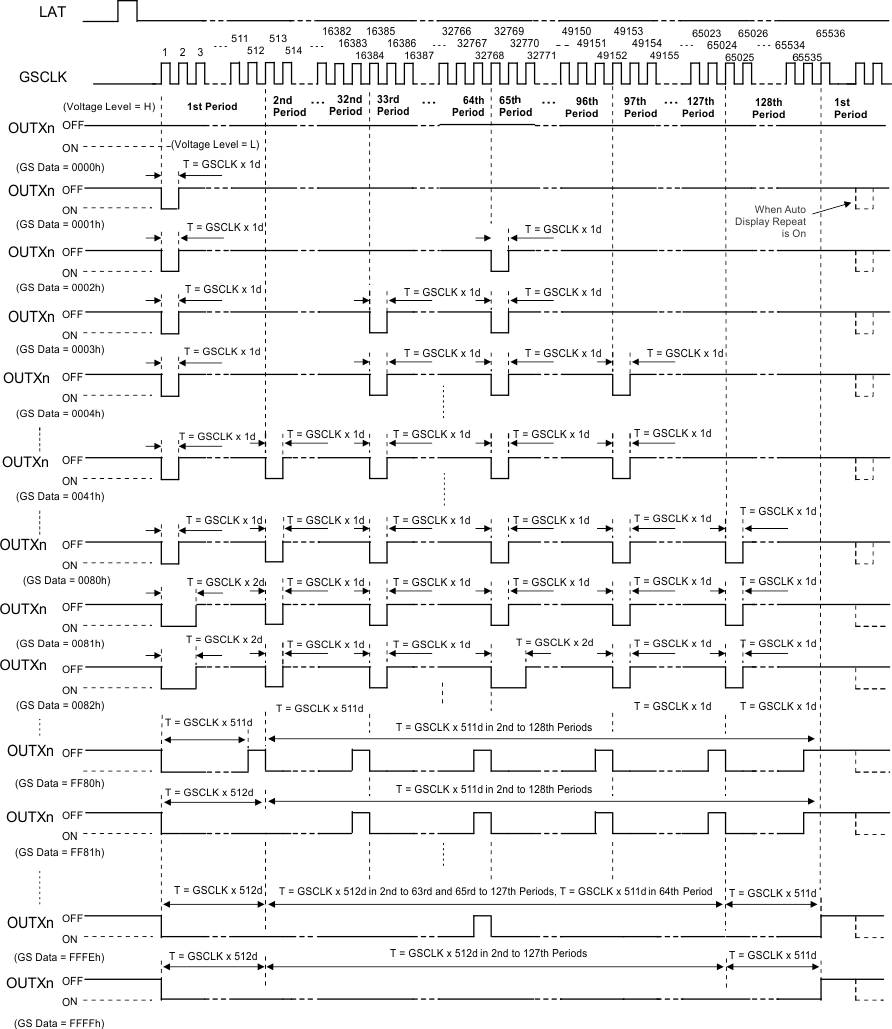 Figure 28. ES PWM Operation
8.4.4.3 Auto Display Repeat Function
This function can repeat the total display period as long as GSCLK is present, as shown in Figure 29. This function is switched on or off by the content of the DSPRPT bit in the control data latch.
When the DSPRPT bit is 1, auto display repeat is enabled and the entire display period repeats. When the DSPRPT bit is 0, auto display repeat is disabled and the entire display period only executes one time after a LAT signal rising edge is input for GS data writes when the display timing reset is enabled.
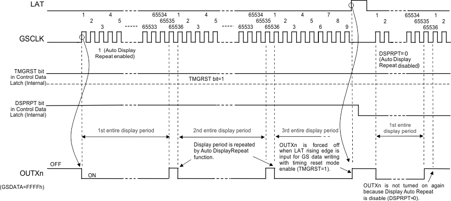 Figure 29. Auto Display Repeat Function
8.4.4.4 Display Timing Reset Function
The display timing reset function allows initializing the display timing with a LAT rising edge. This function can be switched on or off with the TMGRST bit in the control data latch. When the TMGRST bit is 1, the GS counter is reset to 0 and all outputs are forced off at the LAT rising edge for a GS data write. Furthermore, the 768-bit GS data latch is updated with the data from the common shift register and the 336-bit DC data latch is updated with the DC data in the 371-bit control data latch. When the TMGRST bit is 0, the GS counter is not reset and the outputs are not forced off, even if a LAT rising edge is input. A timing diagram for this function is shown in Figure 30.
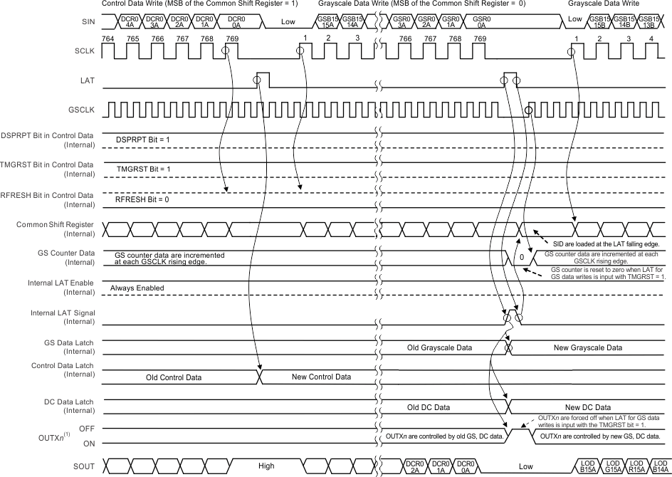 Figure 30. Display Timing Reset Function (DSPRPT = 1, TMGRST = 1, and RFRESH = 0)
8.4.4.5 Auto Data Refresh Function
This function delays updating the grayscale (GS) and dot correction (DC) data until the end of one entire display period. If both DC data and GS data are written by the end of an entire display period, the input DC data are held in the control data latch and the GS data are held in the common shift register. Both DC and GS data are copied to the 336-bit DC data latch and 768-bit GS data latch at the end of an entire display period. The data latches are used for the next display period. GS data are directly copied from the common shift register to the GS data latch. Therefore, GS data must be written after the DC data are written. Furthermore, the GS data in the common shift resistor must not be changed until all data are copied to the GS data latch. Figure 31 and Figure 32 show timing diagrams for this function.
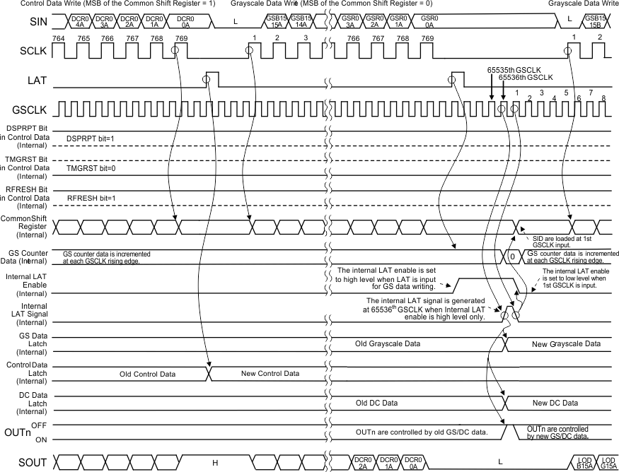 Figure 31. Auto Data Refresh Function 1 (DSPRPT = 1, TMGRST = 0, and RFRESH = 1)
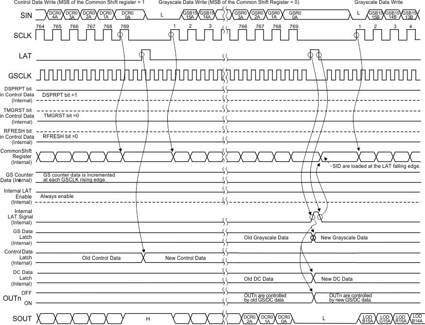 Figure 32. Auto Data Refresh Function 2 (DSPRPT = 1, TMGRST = 0, and RFRESH = 0)