SLLSEE3D August 2013 – April 2016 TLK105L , TLK106L
PRODUCTION DATA.
- 1Device Overview
- 2Revision History
- 3Pin Configuration and Functions
-
4Specifications
- 4.1 Absolute Maximum Ratings
- 4.2 ESD Ratings
- 4.3 Recommended Operating Conditions
- 4.4 20
- 4.5 TLK106L 32-Pin Extended Temperature (105°C) Device Thermal Characteristics
- 4.6 DC Characteristics, VDD_IO
- 4.7 DC Characteristics
- 4.8 Power Supply Characteristics
- 4.9
AC Specifications
- 4.9.1 Power Up Timing
- 4.9.2 Reset Timing
- 4.9.3 MII Serial Management Timing
- 4.9.4 100Mb/s MII Transmit Timing
- 4.9.5 100Mb/s MII Receive Timing
- 4.9.6 100Base-TX Transmit Packet Latency Timing
- 4.9.7 100Base-TX Transmit Packet Deassertion Timing
- 4.9.8 100Base-TX Transmit Timing (tR/F and Jitter)
- 4.9.9 100Base-TX Receive Packet Latency Timing
- 4.9.10 100Base-TX Receive Packet Deassertion Timing
- 4.9.11 10Mbs MII Transmit Timing
- 4.9.12 10Mb/s MII Receive Timing
- 4.9.13 10Base-T Transmit Timing (Start of Packet)
- 4.9.14 10Base-T Transmit Timing (End of Packet)
- 4.9.15 10Base-T Receive Timing (Start of Packet)
- 4.9.16 10Base-T Receive Timing (End of Packet)
- 4.9.17 10Mb/s Jabber Timing
- 4.9.18 10Base-T Normal Link Pulse Timing
- 4.9.19 Auto-Negotiation Fast Link Pulse (FLP) Timing
- 4.9.20 100Base-TX Signal Detect Timing
- 4.9.21 100Mbs Loopback Timing
- 4.9.22 10Mbs Internal Loopback Timing
- 4.9.23 RMII Transmit Timing
- 4.9.24 RMII Receive Timing
- 4.9.25 Isolation Timing
-
5Detailed Description
- 5.1 Hardware Configuration
- 5.2
Architecture
- 5.2.1 100Base-TX Transmit Path
- 5.2.2
100Base-TX Receive Path
- 5.2.2.1 Analog Front End
- 5.2.2.2 Adaptive Equalizer
- 5.2.2.3 Baseline Wander Correction
- 5.2.2.4 NRZI and MLT-3 Decoding
- 5.2.2.5 Descrambler
- 5.2.2.6 5B/4B Decoder and Nibble Alignment
- 5.2.2.7 Timing Loop and Clock Recovery
- 5.2.2.8 Phase-Locked Loops (PLL)
- 5.2.2.9 Link Monitor
- 5.2.2.10 Signal Detect
- 5.2.2.11 Bad SSD Detection
- 5.2.3 10Base-T Receive Path
- 5.2.4 Auto Negotiation
- 5.2.5 Link Down Functionality
- 5.2.6 IEEE 1588 Precision Timing Protocol Support
- 5.3
Register Maps
- 5.3.1
Register Definition
- 5.3.1.1 Basic Mode Control Register (BMCR)
- 5.3.1.2 Basic Mode Status Register (BMSR)
- 5.3.1.3 PHY Identifier Register 1 (PHYIDR1)
- 5.3.1.4 PHY Identifier Register 2 (PHYIDR2)
- 5.3.1.5 Auto-Negotiation Advertisement Register (ANAR)
- 5.3.1.6 Auto-Negotiation Link Partner Ability Register (ANLPAR) (BASE Page)
- 5.3.1.7 Auto-Negotiate Expansion Register (ANER)
- 5.3.1.8 Auto-Negotiate Next Page Transmit Register (ANNPTR)
- 5.3.1.9 Auto-Negotiation Link Partner Ability Next Page Register (ANLNPTR)
- 5.3.1.10 Control register 1 (CR1)
- 5.3.1.11 Control register 2 (CR2)
- 5.3.1.12 Control Register 3 (CR3)
- 5.3.1.13 Extended Register Addressing
- 5.3.1.14 Fast Link Down Status Register
- 5.3.1.15 PHY Status Register (PHYSTS)
- 5.3.1.16 PHY Specific Control Register (PHYSCR)
- 5.3.1.17 MII Interrupt Status Register 1 (MISR1)
- 5.3.1.18 MII Interrupt Status Register 2 (MISR2)
- 5.3.1.19 False Carrier Sense Counter Register (FCSCR)
- 5.3.1.20 Receiver Error Counter Register (RECR)
- 5.3.1.21 BIST Control Register (BISCR)
- 5.3.1.22 RMII Control and Status Register (RCSR)
- 5.3.1.23 LED Control Register (LEDCR)
- 5.3.1.24 PHY Control Register (PHYCR)
- 5.3.1.25 10Base-T Status/Control Register (10BTSCR)
- 5.3.1.26 BIST Control and Status Register 1 (BICSR1)
- 5.3.1.27 BIST Control and Status Register2 (BICSR2)
- 5.3.2 Cable Diagnostic Control Register (CDCR)
- 5.3.3 PHY Reset Control Register (PHYRCR)
- 5.3.4 Multi LED Control register (MLEDCR)
- 5.3.5 Compliance Test register (COMPTR)
- 5.3.6 IEEE1588 Precision Timing Pin Select (PTPPSEL)
- 5.3.7 IEEE1588 Precision Timing Configuration (PTPCFG)
- 5.3.8 TX_CLK Phase Shift Register (TXCPSR)
- 5.3.9 Power Back Off Control Register (PWRBOCR)
- 5.3.10 Voltage Regulator Control Register (VRCR)
- 5.3.11
Cable Diagnostic Configuration/Result Registers
- 5.3.11.1 ALCD Control and Results 1 (ALCDRR1)
- 5.3.11.2 Cable Diagnostic Specific Control Registers (CDSCR1 - CDSCR4)
- 5.3.11.3 Cable Diagnostic Location Results Register 1 (CDLRR1)
- 5.3.11.4 Cable Diagnostic Location Results Register 2 (CDLRR2)
- 5.3.11.5 Cable Diagnostic Location Results Register 3 (DDLRR3)
- 5.3.11.6 Cable Diagnostic Location Results Register 4 (CDLRR4)
- 5.3.11.7 Cable Diagnostic Location Results Register 5 (CDLRR5)
- 5.3.11.8 Cable Diagnostic Amplitude Results Register 1 (CDARR1)
- 5.3.11.9 Cable Diagnostic Amplitude Results Register 2 (CDARR2)
- 5.3.11.10 Cable Diagnostic Amplitude Results Register 3 (CDARR3)
- 5.3.11.11 Cable Diagnostic Amplitude Results Register 4 (CDARR4)
- 5.3.11.12 Cable Diagnostic Amplitude Results Register 5 (CDARR5)
- 5.3.11.13 Cable Diagnostic General Results Register (CDGRR)
- 5.3.11.14 ALCD Control and Results 2 (ALCDRR2)
- 5.3.11.15 ALCD Control and Results 3 (ALCDRR3)
- 5.3.1
Register Definition
- 6Applications, Implementation, and Layout
- 7Device and Documentation Support
- 8Mechanical Packaging and Orderable Information
パッケージ・オプション
メカニカル・データ(パッケージ|ピン)
- RHB|32
サーマルパッド・メカニカル・データ
- RHB|32
発注情報
4 Specifications
All parameters are derived by test, statistical analysis, or design.
4.1 Absolute Maximum Ratings(1)
| MIN | MAX | UNIT | |||
|---|---|---|---|---|---|
| VDD_IO, AVDD33 | Supply voltage | –0.3 | 3.8 | V | |
| PFBIN1, PFBIN2 | –0.3 | 1.8 | |||
| XI | DC Input voltage | –0.3 | 3.8 | V | |
| TD-, TD+, RD-, RD+ | –0.3 | 6 | |||
| Other Inputs | –0.3 | 3.8 | |||
| XO | DC Output voltage | –0.3 | 3.8 | V | |
| Other outputs | –0.3 | 3.8 | |||
| TJ | Maximum die temperature | 125 | °C | ||
| Tstg | Storage temperature | –65 | 150 | °C | |
4.2 ESD Ratings
| VALUE | UNIT | ||||
|---|---|---|---|---|---|
| VESD | Electrostatic discharge (ESD) performance: | Human Body Model (HBM), per ANSI/ESDA/JEDEC JS001(1) | All pins(3) | ±4000 | V |
| Ethernet network pins (TD+, TD–, RD+, RD–)(5) | ±16000 | ||||
| Charged Device Model (CDM), per JESD22-C101(2) |
All pins(4) | ±750 | V | ||
4.3 Recommended Operating Conditions
| MIN | NOM | MAX | UNIT | |||
|---|---|---|---|---|---|---|
| DUAL SUPPLY OPERATION | ||||||
| Core Supply voltage (PFBIN1, PFBIN2) | 1.48 | 1.55 | 1.68 | V | ||
| PD | Power dissipation(2) | 200 | mW | |||
| SINGLE SUPPLY OPERATION | ||||||
| (PFBOUT connected to PFBIN1, PFBIN2 See Figure 5-1) | ||||||
| PD | Power dissipation(1) | 270 | mW | |||
| AVDD33 | Analog 3.3-V Supply | 3.0 | 3.3 | 3.6 | V | |
| VDD_IO | 3.3-V Option | 3.0 | 3.3 | 3.6 | V | |
| 2.5-V Option | 2.25 | 2.5 | 2.75 | |||
| 1.8-V Option (MII Mode only) | 1.62 | 1.8 | 1.98 | |||
| TA | Ambient temperature(3) | TLK105L | –40 | 85 | °C | |
| TLK106L | –40 | 105 | ||||
4.4
4.4.1 TLK105L 32-Pin Industrial Device (85°C) Thermal Characteristics
over operating free-air temperature range (unless otherwise noted)| THERMAL METRIC(1) | TLK105L, TLK106L | UNIT | |
|---|---|---|---|
| RHB (VQFN) | |||
| 32 PINS | |||
| RθJA | Junction-to-ambient thermal resistance | 36.4 | °C/W |
| RθJB | Junction-to-board thermal resistance | 9.3 | °C/W |
| RθJC(top) | Junction-to-case (top) thermal resistance | 26.8 | °C/W |
| RθJC(bot) | Junction-to-case (bottom) thermal resistance | 1.7 | °C/W |
4.5 TLK106L 32-Pin Extended Temperature (105°C) Device Thermal Characteristics
over operating free-air temperature range (unless otherwise noted)| THERMAL METRIC(1) | TLK105L, TLK106L | UNIT | |
|---|---|---|---|
| RHB (VQFN) | |||
| 32 PINS | |||
| RθJA | Junction-to-ambient thermal resistance (no airflow), JEDEC high-K model | 36.4 | °C/W |
| RθJB | Junction-to-board thermal resistance | 9.3 | °C/W |
| RθJC(top) | Junction-to-case (top) thermal resistance | 26.8 | °C/W |
| RθJC(bot) | Junction-to-case (bottom) thermal resistance | 1.7 | °C/W |
4.6 DC Characteristics, VDD_IO
over operating free-air temperature range (unless otherwise noted)| PARAMETER | TEST CONDITIONS | MIN | TYP | MAX | UNIT | ||
|---|---|---|---|---|---|---|---|
| 3.3V VDD_IO | |||||||
| VIH | Input high voltage | Nominal VCC = 3.3V | VDD_IO = 3.3 V ±10% | 2.0 | V | ||
| VIL | Input low voltage | VDD_IO = 3.3 V±10% | 0.8 | V | |||
| VOL | Output low voltage | IOL = 4 mA | VDD_IO = 3.3 V±10% | 0.4 | V | ||
| VOH | Output high voltage | IOH = –4 mA | VDD_IO = 3.3 V±10% | VDD_IO – 0.5 | V | ||
| 2.5V VDD_IO | |||||||
| VIH | Input high voltage | VDD_IO = 2.5 V±10% | 1.5 | V | |||
| VIL | Input low voltage | VDD_IO = 2.5 V±10% | 0.5 | V | |||
| VOL | Output low voltage | IOL = 2 mA | VDD_IO = 2.5 V±10% | 0.4 | V | ||
| VOH | Output high voltage | IOH = –2 mA | VDD_IO = 2.5 V±10% | VDD_IO – 0.4 | V | ||
| 1.8V VDD_IO | |||||||
| VIH | Input high voltage | VDD_IO = 1.8 V±10% | 1.3 | V | |||
| VIL | Input low voltage | VDD_IO = 1.8 V±10% | 0.45 | V | |||
| VOL | Output low voltage | IOL = 2 mA | VDD_IO = 1.8 V±10% | 0.4 | V | ||
| VOH | Output high voltage | IOH = –2 mA | VDD_IO = 1.8 V±10% | VDD_IO – 0.4 | V | ||
4.7 DC Characteristics
over operating free-air temperature range (unless otherwise noted)| PARAMETER | TEST CONDITIONS | MIN | TYP | MAX | UNIT | ||
|---|---|---|---|---|---|---|---|
| IIH | Input high current | VIN = VCC | 10 | μA | |||
| IIL | Input low current | VIN = GND | 10 | μA | |||
| IOZ | 3-State leakage | VOUT = VCC, VOUT = GND | ±10 | μA | |||
| RPULLUP | Integrated Pullup Resistance | 14.7 | 23.7 | 49.7 | kΩ | ||
| RPULLDOWN | Integrated Pulldown Resistance | 14.5 | 24.9 | 48.1 | kΩ | ||
| VTPTD_100 | 100M transmit voltage | 0.95 | 1 | 1.05 | V | ||
| VTPTDsym | 100M transmit voltage symmetry | ±2% | |||||
| VTPTD_10 | 10M transmit voltage | 2.2 | 2.5 | 2.8 | V | ||
| CIN1 | CMOS input capacitance | 5 | pF | ||||
| COUT1 | CMOS output capacitance | 5 | pF | ||||
| VTH1 | 10Base-T Receive threshold | 200 | mV | ||||
4.8 Power Supply Characteristics
The data was measured using a TLK10xL evaluation board. The current from each of the power supplies is measured and the power dissipation is computed. For the single 3.3-V external supply case the power dissipation across the internal linear regulator is also included. All the power dissipation numbers are measured at the nominal power supply and typical temperature of 25°C. The power needed is given both for the device only, and including the center tap of the transformer for a total system power requirement. The center tap of the transformer is normally connected to the 3.3-V supply, thus the current needed may also be easily calculated.
4.8.1 Active Power, Single Supply Operation
| PARAMETER | TEST CONDITIONS | FROM POWER PINS | FROM TRANSFORMER CENTER TAP |
UNIT |
|---|---|---|---|---|
| 100Base-TX /W Traffic (full packet 1518B rate) | Single 3.3-V external supply | 203 | 73 | mW |
| 10Base-T /W Traffic (full packet 1518B rate) | 96 | 211 |
4.8.2 Active Power, Dual Supply Operation
| PARAMETER | TEST CONDITIONS | FROM 3.3-V POWER | FROM 1.55 V PFBIN1, PFBIN2 |
FROM TRANSFORMER CENTER TAP |
UNIT |
|---|---|---|---|---|---|
| 100Base-TX /W Traffic (full packet 1518B rate) | Dual external supplies, 3.3 V and 1.55 V |
53 | 73 | 73 | mW |
| 10Base-T /W Traffic (full packet 1518B rate) | 23 | 35 | 212 |
4.8.3 Power-Down Power
| PARAMETER | TEST CONDITIONS(1) | FROM 3.3-V POWER | FROM 1.55 V PFBIN1, PFBIN2 |
FROM TRANSFORMER CENTER TAP | UNIT |
|---|---|---|---|---|---|
| IEEE PWDN | Single 3.3-V external supply | 12 | – | 5 | mW |
| Passive Sleep Mode | 71 | – | 5 | ||
| Active Sleep Mode | 71 | – | 5 | ||
| IEEE PWDN | Dual external supplies, 3.3 V and 1.55 V |
12 | 0 | 5 | |
| Passive Sleep Mode | 21 | 23 | 5 | ||
| Active Sleep Mode | 21 | 23 | 5 |
4.9 AC Specifications
4.9.1 Power Up Timing
Table 4-1 Power Up Timing
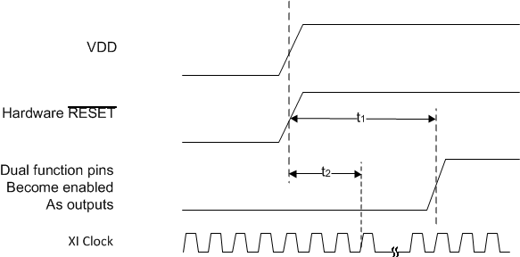 Figure 4-1 Power Up Timing
NOTE
It is important to choose pullup and-or pulldown resistors for each of the hardware configuration pins that provide fast RC time constants in order to latch in the proper value prior to the pin transitioning to an output driver.
4.9.2 Reset Timing
Table 4-2 Reset Timing
| PARAMETER | TEST CONDITIONS | MIN | TYP | MAX | UNIT | |
|---|---|---|---|---|---|---|
| t1 | RESET pulse width | XI Clock must be stable for minimum of 1µs during RESET pulse low time. | 1 | µs | ||
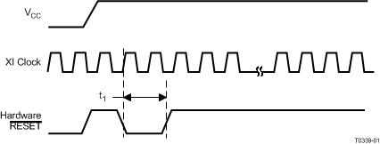 Figure 4-2 Reset Timing
4.9.3 MII Serial Management Timing
Table 4-3 MII Serial Management Timing
| PARAMETER | TEST CONDITIONS | MIN | TYP | MAX | UNIT | |
|---|---|---|---|---|---|---|
| t1 | MDC Frequency | 2.5 | 25 | MHz | ||
| t2 | MDC to MDIO (Output) Delay Time | 0 | 30 | ns | ||
| t3 | MDIO (Input) to MDC Hold Time | 10 | ns | |||
| t4 | MDIO (Input) to MDC Setup Time | 10 | ns | |||
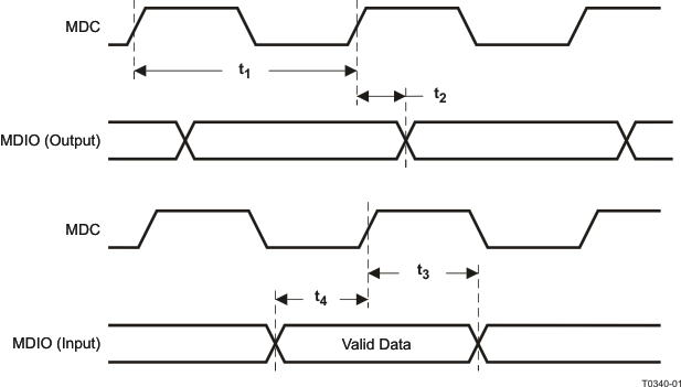 Figure 4-3 MII Serial Management Timing
4.9.4 100Mb/s MII Transmit Timing
Table 4-4 100Mb/s MII Transmit Timing
| PARAMETER | TEST CONDITIONS | MIN | TYP | MAX | UNIT | |
|---|---|---|---|---|---|---|
| t1 | TX_CLK High Time | 100Mbs Normal mode | 16 | 20 | 24 | ns |
| t2 | TX_CLK Low Time | |||||
| t3 | TXD[3:0], TX_EN Data Setup to TX_CLK | 100Mbs Normal mode | 10 | ns | ||
| t4 | TXD[3:0], TX_EN Data Hold from TX_CLK | 100Mbs Normal mode | 0 | ns | ||
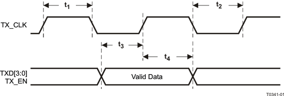 Figure 4-4 100Mb/s MII Transmit Timing
4.9.5 100Mb/s MII Receive Timing
Table 4-5 100Mb/s MII Receive Timing
| PARAMETER(1) | TEST CONDITIONS | MIN | TYP | MAX | UNIT | |
|---|---|---|---|---|---|---|
| t1 | RX_CLK High Time | 100Mbs Normal mode | 16 | 20 | 24 | ns |
| t2 | RX_CLK Low Time | |||||
| t3 | RX_CLK to RXD[3:0], RX_DV, RX_ER Delay | 100Mbs Normal mode | 10 | 30 | ns | |
 Figure 4-5 100Mb/s MII Receive Timing
4.9.6 100Base-TX Transmit Packet Latency Timing
Table 4-6 100Base-TX Transmit Packet Latency Timing
| PARAMETER | TEST CONDITIONS | MIN | TYP | MAX | UNIT | |
|---|---|---|---|---|---|---|
| t1 | TX_CLK to PMD Output Pair Latency | 100Mbs Normal mode(1) | 4.8 | bits(2) | ||
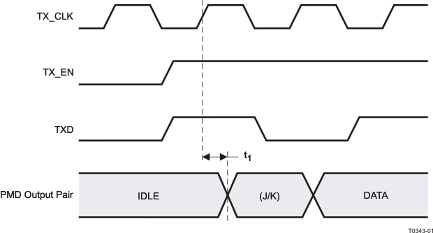 Figure 4-6 100Base-TX Transmit Packet Latency Timing
4.9.7 100Base-TX Transmit Packet Deassertion Timing
Table 4-7 100Base-TX Transmit Packet Deassertion Timing
| PARAMETER | TEST CONDITIONS | MIN | TYP | MAX | UNIT | |
|---|---|---|---|---|---|---|
| t1 | TX_CLK to PMD Output Pair deassertion | 100Mbs Normal mode | 4.6 | bits | ||
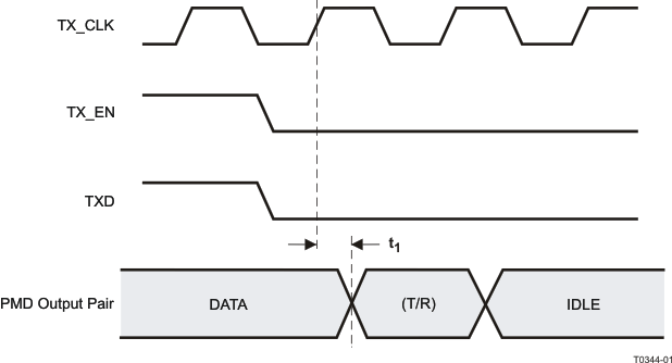 Figure 4-7 100Base-TX Transmit Packet Deassertion Timing
4.9.8 100Base-TX Transmit Timing (tR/F and Jitter)
Table 4-8 100Base-TX Transmit Timing (tR/F and Jitter)
| PARAMETER | TEST CONDITIONS | MIN | TYP | MAX | UNIT | |
|---|---|---|---|---|---|---|
| t1 | 100Mbs PMD Output Pair tR and tF (1) | 3 | 4 | 5 | ns | |
| 100Mbs tR and tF Mismatch(2) | 500 | ps | ||||
| t2 | 100Mbs PMD Output Pair Transmit Jitter | 1.4 | ns | |||
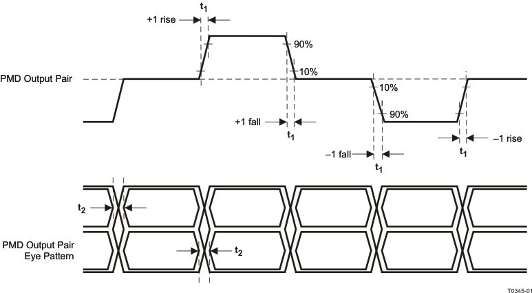 Figure 4-8 100Base-TX Transmit Timing (tR/F and Jitter)
4.9.9 100Base-TX Receive Packet Latency Timing
Table 4-9 100Base-TX Receive Packet Latency Timing
| PARAMETER | TEST CONDITIONS(3) | MIN | TYP | MAX | UNIT(2) | |
|---|---|---|---|---|---|---|
| t1 | Carrier Sense ON Delay(1) | 100Mbs normal mode | 14 | bits | ||
| t2 | Receive Data Latency | 100Mbs normal mode | 19 | |||
| t2 | Receive Data Latency(4) | 100Mbs normal mode with fast RXDV detection ON | 15 | |||
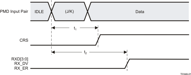 Figure 4-9 100Base-TX Receive Packet Latency Timing
4.9.10 100Base-TX Receive Packet Deassertion Timing
Table 4-10 100Base-TX Receive Packet Deassertion Timing
| PARAMETER | TEST CONDITIONS | MIN | TYP | MAX | UNIT | |
|---|---|---|---|---|---|---|
| t1 | Carrier Sense OFF Delay(1) | 100Mbs Normal mode | 19 | bits(2) | ||
 Figure 4-10 100Base-TX Receive Packet Deassertion Timing
4.9.11 10Mbs MII Transmit Timing
Table 4-11 10Mbs MII Transmit Timing
| PARAMETER | TEST CONDITIONS | MIN | TYP | MAX | UNIT | |
|---|---|---|---|---|---|---|
| t1 | TX_CLK Low Time | 10Mbs MII mode | 190 | 200 | 210 | ns |
| t2 | TX_CLK High Time | |||||
| t3 | TXD[3:0], TX_EN Data Setup to TX_CLK ↑ | 10Mbs MII mode | 25 | ns | ||
| t4 | TXD[3:0], TX_EN Data Hold from TX_CLK ↑ | 10Mbs MII mode | 0 | ns | ||
An attached Mac should drive the transmit signals using the positive edge of TX_CLK. As shown in Figure 4-11, the MII signals are sampled on the falling edge of TX_CLK.
 Figure 4-11 10Mbs MII Transmit Timing
4.9.12 10Mb/s MII Receive Timing
Table 4-12 10Mb/s MII Receive Timing
| PARAMETER(1) | TEST CONDITIONS | MIN | TYP | MAX | UNIT | |
|---|---|---|---|---|---|---|
| t1 | RX_CLK High Time | 160 | 200 | 240 | ns | |
| t2 | RX_CLK Low Time | |||||
| t3 | RX_CLK rising edge delay from RXD[3:0], RX_DV Valid | 10Mbs MII mode | 100 | ns | ||
| t4 | RX_CLK to RXD[3:0], RX_DV Delay | 10Mbs MII mode | 100 | ns | ||
 Figure 4-12 10Mb/s MII Receive Timing
4.9.13 10Base-T Transmit Timing (Start of Packet)
Table 4-13 10Base-T Transmit Timing (Start of Packet)
| PARAMETER | TEST CONDITIONS | MIN | TYP | MAX | UNIT(1) | |
|---|---|---|---|---|---|---|
| t1 | Transmit Output Delay from the Falling Edge of TX_CLK | 10Mbs MII mode | 5.8 | bits | ||
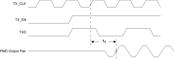 Figure 4-13 10Base-T Transmit Timing (Start of Packet)
4.9.14 10Base-T Transmit Timing (End of Packet)
Table 4-14 10Base-T Transmit Timing (End of Packet)
| PARAMETER | TEST CONDITIONS | MIN | TYP | MAX | UNIT | |
|---|---|---|---|---|---|---|
| t1 | End of Packet High Time (with ‘0’ ending bit) | 250 | 310 | ns | ||
| t2 | End of Packet High Time (with ‘1’ ending bit) | 250 | 310 | ns | ||
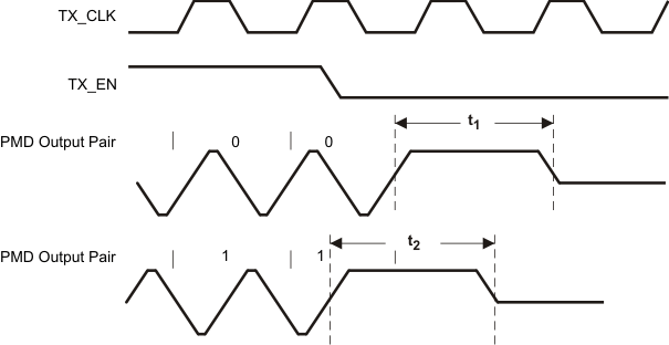 Figure 4-14 10Base-T Transmit Timing (End of Packet)
4.9.15 10Base-T Receive Timing (Start of Packet)
Table 4-15 10Base-T Receive Timing (Start of Packet)
| PARAMETER | TEST CONDITIONS | MIN | TYP | MAX | UNIT | |
|---|---|---|---|---|---|---|
| t1 | Carrier Sense Turn On Delay (PMD Input Pair to CRS) | 550 | 1000 | ns | ||
| t2 | RX_DV Latency(1) | 14 | bits | |||
| t3 | Receive Data Latency | Measurement shown from SFD | 14 | bits | ||
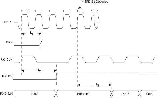 Figure 4-15 10Base-T Receive Timing (Start of Packet)
4.9.16 10Base-T Receive Timing (End of Packet)
Table 4-16 10Base-T Receive Timing (End of Packet)
| PARAMETER | TEST CONDITIONS | MIN | TYP | MAX | UNIT | |
|---|---|---|---|---|---|---|
| t1 | Carrier Sense Turn Off Delay | 1.8 | μs | |||
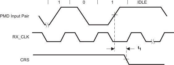 Figure 4-16 10Base-T Receive Timing (End of Packet)
4.9.17 10Mb/s Jabber Timing
Table 4-17 10Mb/s Jabber Timing
| PARAMETER | TEST CONDITIONS | MIN | TYP | MAX | UNIT | |
|---|---|---|---|---|---|---|
| t1 | Jabber Activation Time | 10 Mb/s MII mode | 100 | ms | ||
| t2 | Jabber Deactivation Time | 500 | ||||
 Figure 4-17 10Mb/s Jabber Timing
4.9.18 10Base-T Normal Link Pulse Timing
Table 4-18 10Base-T Normal Link Pulse Timing
| PARAMETER(1) | TEST CONDITIONS | MIN | TYP | MAX | UNIT | |
|---|---|---|---|---|---|---|
| t1 | Pulse Period | 10 Mb/s MII mode | 16 | ms | ||
| t2 | Pulse Width | 100 | ns | |||
 Figure 4-18 10Base-T Normal Link Pulse Timing
4.9.19 Auto-Negotiation Fast Link Pulse (FLP) Timing
Table 4-19 Auto-Negotiation Fast Link Pulse (FLP) Timing
| PARAMETER | TEST CONDITIONS | MIN | TYP | MAX | UNIT | |
|---|---|---|---|---|---|---|
| t1 | Clock Pulse to Clock Pulse Period | 125 | μs | |||
| t2 | Clock Pulse to Data Pulse Period | Data = 1 | 62 | μs | ||
| t3 | Clock, Data Pulse Width | 114 | ns | |||
| t4 | FLP Burst to FLP Burst Period | 16 | ms | |||
| t5 | Burst Width | 2 | ms | |||
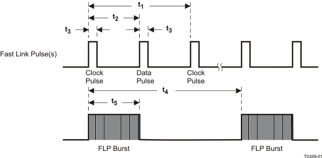 Figure 4-19 Auto-Negotiation Fast Link Pulse (FLP) Timing
4.9.20 100Base-TX Signal Detect Timing
Table 4-20 100Base-TX Signal Detect Timing
| PARAMETER | TEST CONDITIONS | MIN | TYP | MAX | UNIT | |
|---|---|---|---|---|---|---|
| t1 | SD Internal Turn-on Time | 100 | μs | |||
| t2 | Internal Turn-off Time | 200 | μs | |||

NOTE:
The signal amplitude on PMD Input Pair must be TP-PMD compliant.4.9.21 100Mbs Loopback Timing
Table 4-21 100Mbs Loopback Timing
| PARAMETER | TEST CONDITIONS | MIN | TYP | MAX | UNIT | |
|---|---|---|---|---|---|---|
| t1 | TX_EN to RX_DV Loopback | 100Mbs external loopback | 241 | 242 | 243 | ns |
| 100Mbs external loopback – fast RX_DV mode | 201 | 202 | 203 | |||
| 100Mbs analog loopback | 232 | 233 | 234 | |||
| 100Mbs PCS Input loop back | 120 | 121 | 122 | |||
| 100Mbs MII loop back | 8 | 9 | 10 | |||
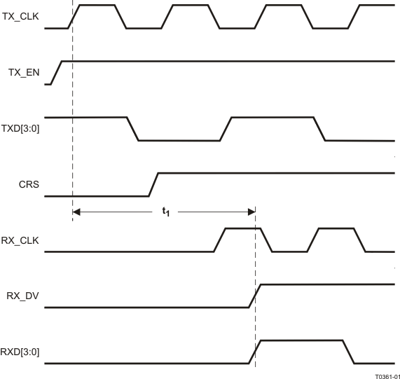
4.9.22 10Mbs Internal Loopback Timing
Table 4-22 10Mbs Internal Loopback Timing
| PARAMETER | TEST CONDITIONS | MIN | TYP | MAX | UNIT | |
|---|---|---|---|---|---|---|
| t1 | TX_EN to RX_DV Loopback | 10Mbs internal loopback mode | 1.7 | μs | ||
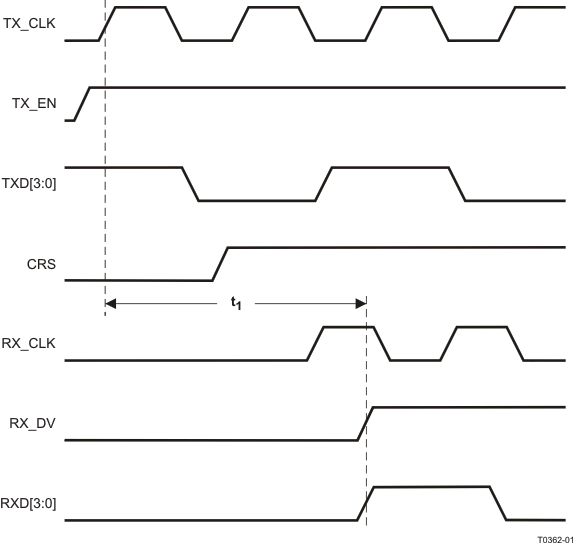
4.9.23 RMII Transmit Timing
Table 4-23 RMII Transmit Timing
| PARAMETER | TEST CONDITIONS | MIN | TYP | MAX | UNIT | |
|---|---|---|---|---|---|---|
| t1 | XI Clock Period | 50MHz Reference Clock | 20 | ns | ||
| t2 | TXD[1:0] and TX_EN data setup to X1 rising | 1.4 | ||||
| t3 | TXD[1:0] and TX_EN data hold to X1 rising | VDD_IO = 3.3V | 2.0 | |||
| VDD_IO = 2.5V | 4.9 | |||||
| t4 | XI Clock to PMD Output Pair Latency | 12 | bits | |||
 Figure 4-23 RMII Transmit Timing
4.9.24 RMII Receive Timing
Table 4-24 RMII Receive Timing
| PARAMETER | TEST CONDITIONS | MIN | TYP | MAX | UNIT | |
|---|---|---|---|---|---|---|
| t1 | XI Clock Period | 50MHz Reference Clock | 20 | ns | ||
| t2 | RXD[1:0], CRS_DV, RX_DV and RX_ER output delay from XI rising | 4 | 10.8 | 14 | ||
| t3 | CRS ON delay | From JK symbol on PMD Receive Pair to initial assertion of CRS_DV | 17.6 | bits | ||
| t4 | CRS OFF delay | From TR symbol on PMD Receive Pair to initial assertion of CRS_DV | 26.2 | |||
| t5 | RXD[1:0] and RX_ER latency | From symbol on Receive Pair. * Elasticity buffer set to default value (01) | 29.7 | |||
| t6 | RX_CLK Clock Period | 50MHz “Recovered clock” while working in “RMII receive clock” mode | 20 | ns | ||
| t7 | RXD[1:0], CRS_DV, RX_DV and RX_ER output delay from RX_CLK rising | While working in “RMII receive clock” mode | 3.8 | |||
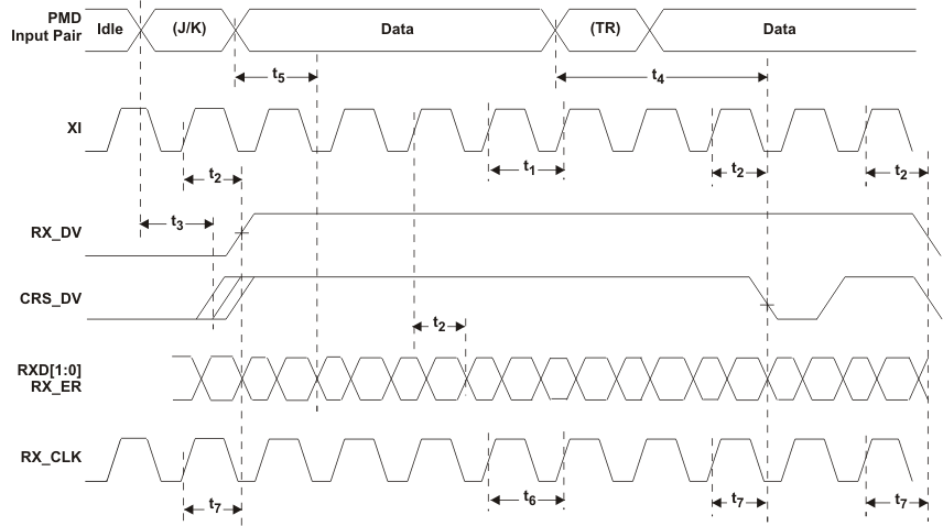 Figure 4-24 RMII Receive Timing
NOTE
- Per the RMII Specification, output delays assume a 25pF load.
- CRS_DV is asserted asynchronously in order to minimize latency of control signals through the PHY. CRS_DV may toggle synchronously at the end of the packet to indicate CRS de-assertion.
- RX_DV is synchronous to XI. While not part of the RMII specification, this signal is provided to simplify recovery of receive data.
- “RMII receive clock” mode is not part of the RMII specification that allows synchronization of the MAC-PHY RX interface in RMII mode. Setting register 0x000A bit [0] is required to activate this mode.
4.9.25 Isolation Timing
Table 4-25 Isolation Timing
| PARAMETER | TEST CONDITIONS | MIN | TYP | MAX | UNIT | |
|---|---|---|---|---|---|---|
| t1 | From Deassertion of S/W or H/W Reset to transition from Isolate to Normal mode | 71 | ns | |||
 Figure 4-25 Isolation Timing