JAJSE11B November 2015 – September 2017 TLV1701-Q1 , TLV1702-Q1 , TLV1704-Q1
PRODUCTION DATA.
- 1 特長
- 2 アプリケーション
- 3 概要
- 4 改訂履歴
- 5 Device Comparison Table
- 6 Pin Configuration and Functions
- 7 Specifications
- 8 Detailed Description
- 9 Application and Implementation
- 10Power Supply Recommendations
- 11Layout
- 12デバイスおよびドキュメントのサポート
- 13メカニカル、パッケージ、および注文情報
パッケージ・オプション
メカニカル・データ(パッケージ|ピン)
サーマルパッド・メカニカル・データ
発注情報
9 Application and Implementation
NOTE
Information in the following applications sections is not part of the TI component specification, and TI does not warrant its accuracy or completeness. TI’s customers are responsible for determining suitability of components for their purposes. Customers should validate and test their design implementation to confirm system functionality.
9.1 Application Information
The TLV170x-Q1 device can be used in a wide variety of applications, such as zero crossing detectors, window comparators, over and undervoltage detectors, and high-side voltage sense circuits.
9.2 Typical Application
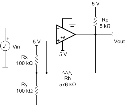
Comparators are used to differentiate between two different signal levels. For example, a comparator differentiates between an overtemperature and normal-temperature condition. However, noise or signal variation at the comparison threshold causes multiple transitions. This application example sets upper and lower hysteresis thresholds to eliminate the multiple transitions caused by noise.
 Figure 20. Comparator Schematic With Hysteresis
9.2.1 Design Requirements
The design requirements are as follows:
- Supply voltage: 5 V
- Input: 0 V to 5 V
- Lower threshold (VL) = 2.3 V ±0.1 V
- Upper threshold (VH) = 2.7 V ±0.1 V
- VH – VL = 2.4 V ±0.1 V
- Low-power consumption
9.2.2 Detailed Design Procedure
Make a small change to the comparator circuit to add hysteresis. Hysteresis uses two different threshold voltages to avoid the multiple transitions introduced in the previous circuit. The input signal must exceed the upper threshold (VH) to transition low, or below the lower threshold (VL) to transition high.
Figure 20 illustrates hysteresis on a comparator. Resistor Rh sets the hysteresis level. An open-collector output stage requires a pullup resistor (Rp). The pullup resistor creates a voltage divider at the comparator output that introduces an error when the output is at logic high. This error can be minimized if Rh > 100 Rp.
When the output is at a logic high (5 V), Rh is in parallel with Rx (ignoring Rp). This configuration drives more current into Ry, and raises the threshold voltage (VH) to 2.7 V. The input signal must drive above VH = 2.7 V to cause the output to transition to logic low (0 V).
When the output is at logic low (0 V), Rh is in parallel with Ry. This configuration reduces the current into Ry, and reduces the threshold voltage to 2.3 V. The input signal must drive below VL = 2.3 V to cause the output to transition to logic high (5 V).
For more details on this design and other alternative devices that can be used in place of the TLV1702, refer to Precision Design TIPD144, Comparator with Hysteresis Reference Design.
9.2.3 Application Curve
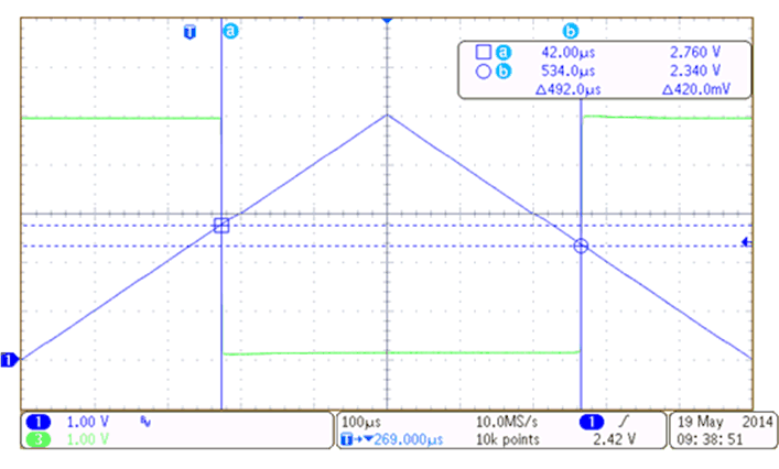
Figure 21 shows the upper and lower thresholds for hysteresis. The upper threshold is 2.76 V and the lower threshold is 2.34 V, both of which are close to the design target.
 Figure 21. TLV1701 Upper and Lower Threshold With Hysteresis