JAJSGX9B August   2018  – January 2020 TLV1805-Q1

PRODUCTION DATA.  

  1. 特長
  2. アプリケーション
  3. 概要
    1.     Device Images
      1.      N チャネル MOSFET による逆電流保護
      2.      P チャネル MOSFET による逆電流および過電圧保護
  4. 改訂履歴
  5. Pin Configuration and Functions
    1.     Pin Functions
  6. Specifications
    1. 6.1 Absolute Maximum Ratings
    2. 6.2 ESD Ratings
    3. 6.3 Recommended Operating Conditions
    4. 6.4 Thermal Information
    5. 6.5 Electrical Characteristics
    6. 6.6 Switching Characteristics
    7. 6.7 Typical Characteristics
  7. Detailed Description
    1. 7.1 Overview
    2. 7.2 Functional Block Diagram
    3. 7.3 Feature Description
      1. 7.3.1 Rail to Rail Inputs
      2. 7.3.2 Power On Reset
      3. 7.3.3 High Power Push-Pull Output
      4. 7.3.4 Shutdown Function
      5. 7.3.5 Internal Hysteresis
    4. 7.4 Device Functional Modes
      1. 7.4.1 External Hysteresis
        1. 7.4.1.1 Inverting Comparator With Hysteresis
        2. 7.4.1.2 Noninverting Comparator With Hysteresis
  8. Application and Implementation
    1. 8.1 Application Information
    2. 8.2 Typical Applications
      1. 8.2.1 Design Requirements
      2. 8.2.2 Detailed Design Procedure
      3. 8.2.3 Application Curve
      4. 8.2.4 Reverse Current Protection Using MOSFET and TLV1805-Q1
        1. 8.2.4.1 Minimum Reverse Current
        2. 8.2.4.2 N-Channel Reverse Current Protection Circuit
          1. 8.2.4.2.1 N-Channel Oscillator Circuit
      5. 8.2.5 P-Channel Reverse Current Protection Circuit
      6. 8.2.6 P-Channel Reverse Current Protection With Overvotlage Protection
      7. 8.2.7 ORing MOSFET Controller
  9. Power Supply Recommendations
  10. 10Layout
    1. 10.1 Layout Guidelines
    2. 10.2 Layout Example
  11. 11デバイスおよびドキュメントのサポート
    1. 11.1 ドキュメントのサポート
      1. 11.1.1 関連資料
    2. 11.2 ドキュメントの更新通知を受け取る方法
    3. 11.3 サポート・リソース
    4. 11.4 商標
    5. 11.5 静電気放電に関する注意事項
    6. 11.6 Glossary
  12. 12メカニカル、パッケージ、および注文情報

パッケージ・オプション

メカニカル・データ(パッケージ|ピン)
サーマルパッド・メカニカル・データ
発注情報

Typical Characteristics

at TA = 25°C, VS = 12 V, VCM = VS/2, and input overdrive = 100 mV (unless otherwise noted)
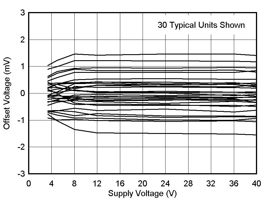
TLV1805-Q1 VIO_vs_VS.gif
Figure 3. Input Offset Voltage vs. Supply Voltage
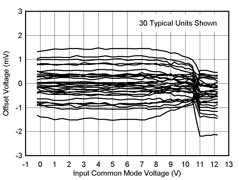
TLV1805-Q1 VIO_vs_VCM.gif
Figure 5. Offset Voltage vs. Common Mode
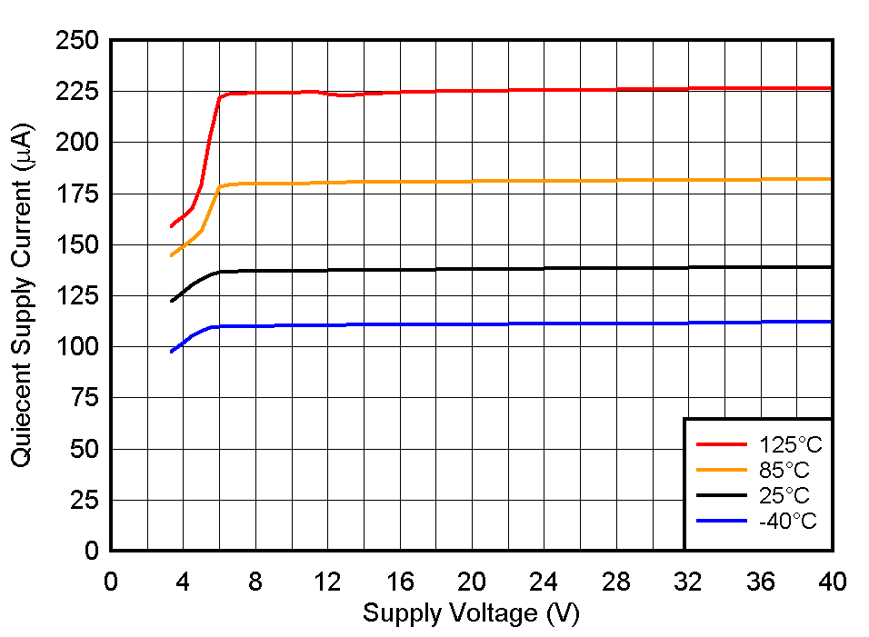
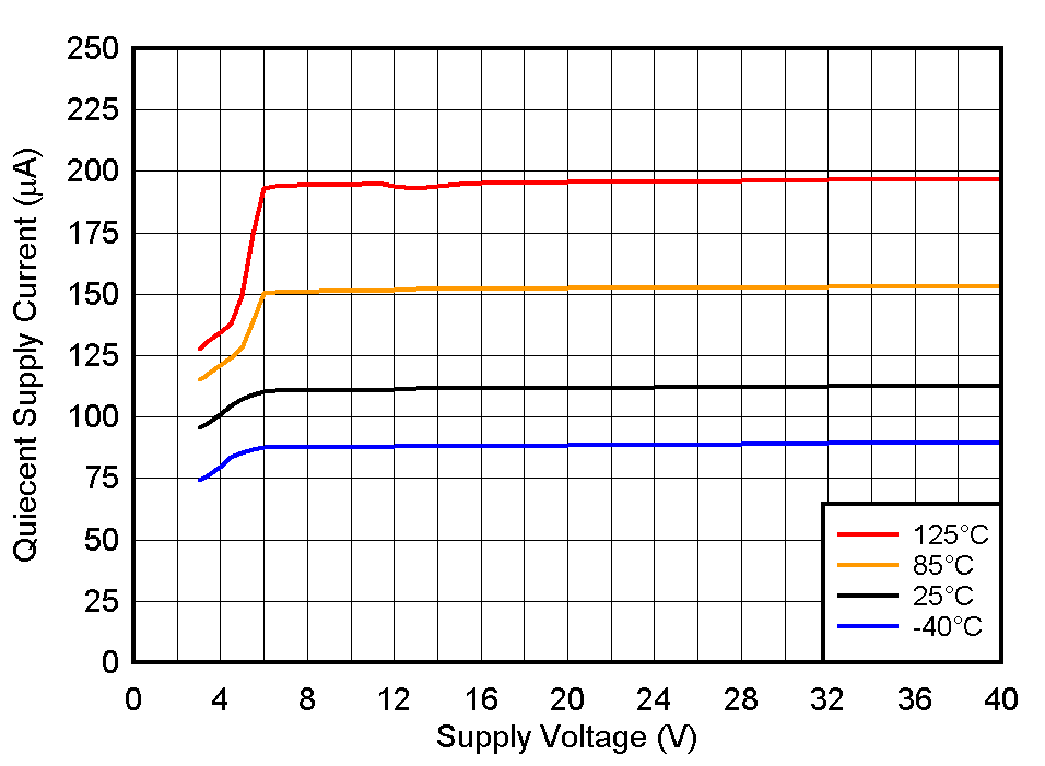
TLV1805-Q1 IQ_vs_VS.gif
VCM = V- Output Low (VID = -0.1 V)
Figure 7. Supply Current vs. Supply Voltage, Output Low
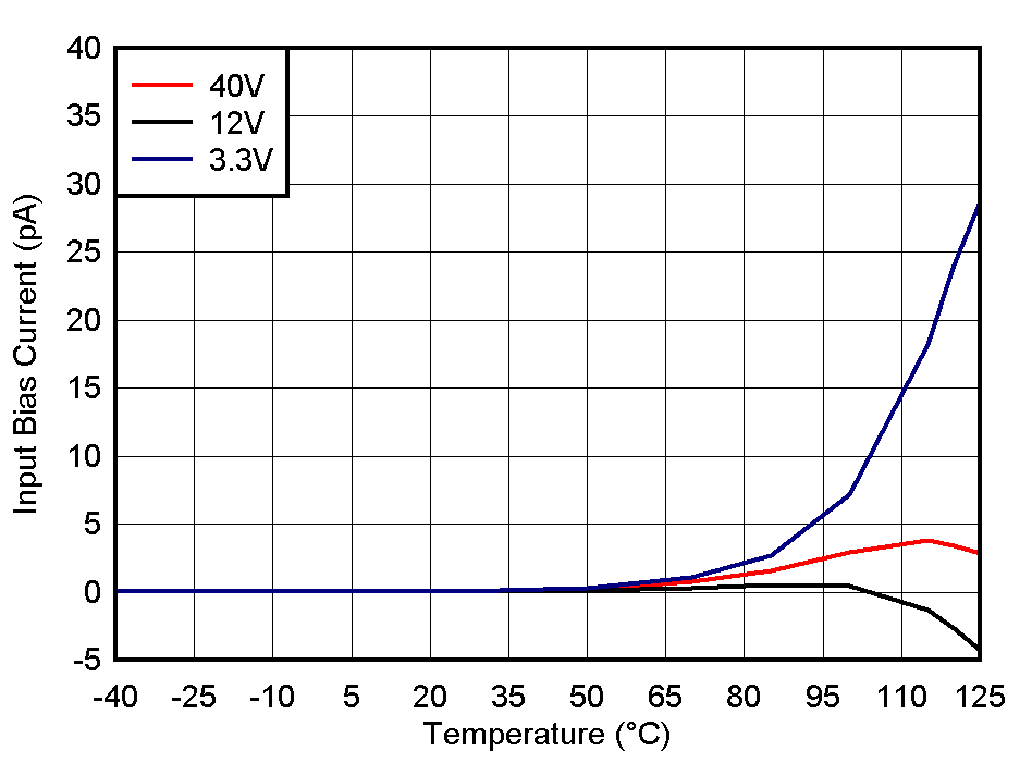
TLV1805-Q1 IB_vs_TA.gif
Figure 9. Input Bias Current vs. Temperature
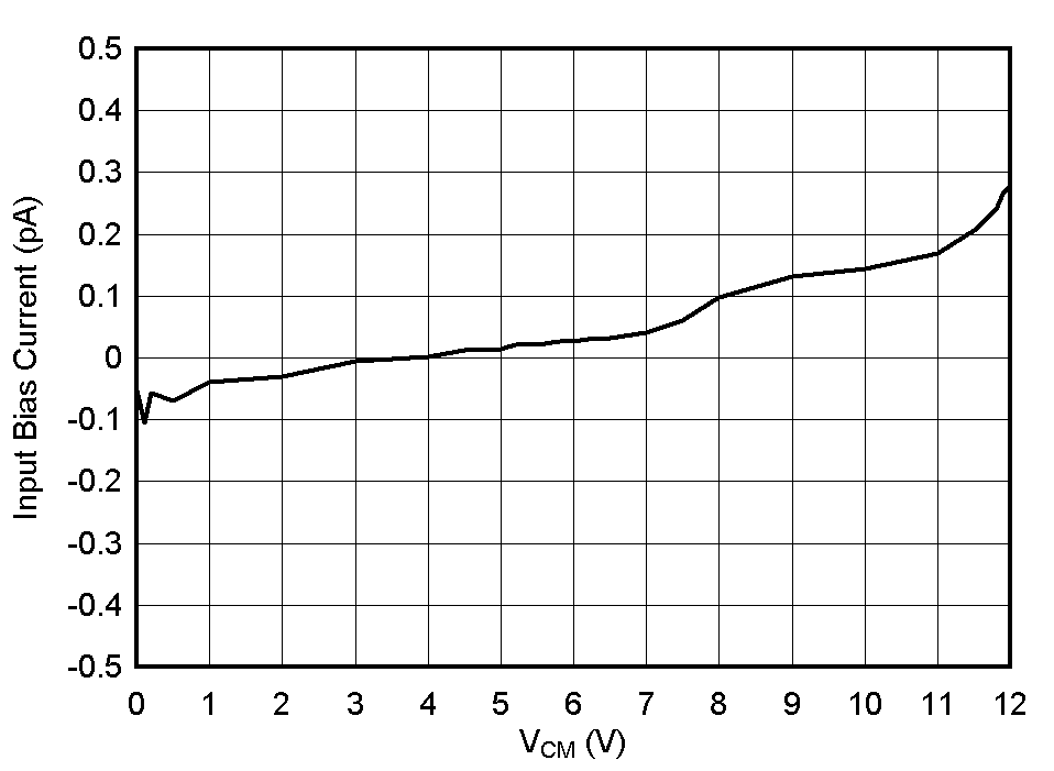
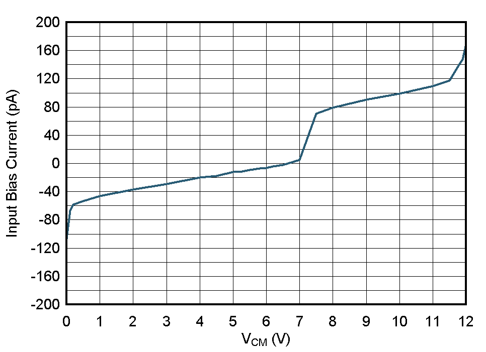
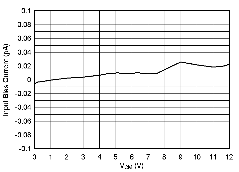
TLV1805-Q1 IB_vs_VCM_25C.gif
TA = 25 °C
Figure 11. Input Bias Current vs. Common Mode, 25°C
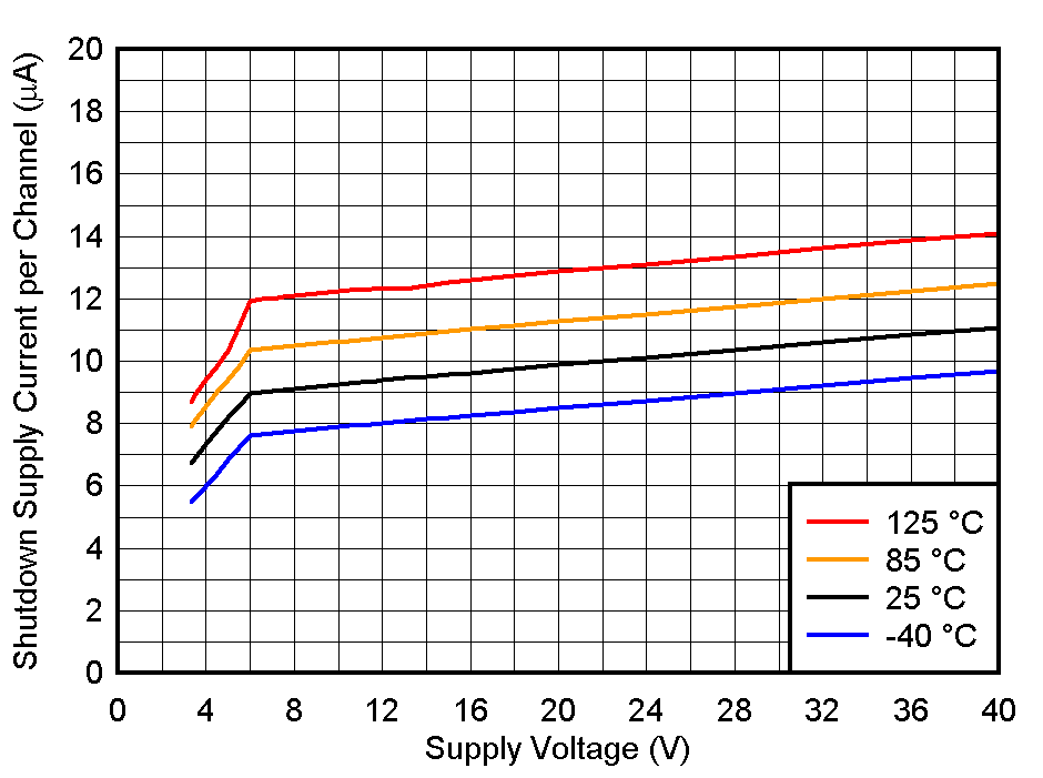
TLV1805-Q1 IQsd_vs_VS.gif
VCM = V-
Figure 13. Shutdown Supply Current vs. Supply Votlage
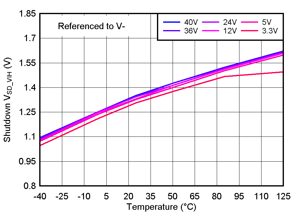
TLV1805-Q1 SDVHI_vs_TA.gif
Figure 15. Shutdown Voltage High Threshold vs. Temperature
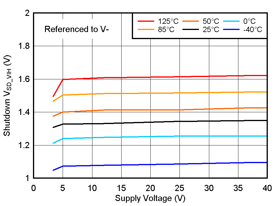
TLV1805-Q1 SDVHI_vs_VS.gif
Figure 17. Shutdown Voltage High Threshold vs. Supply Voltage
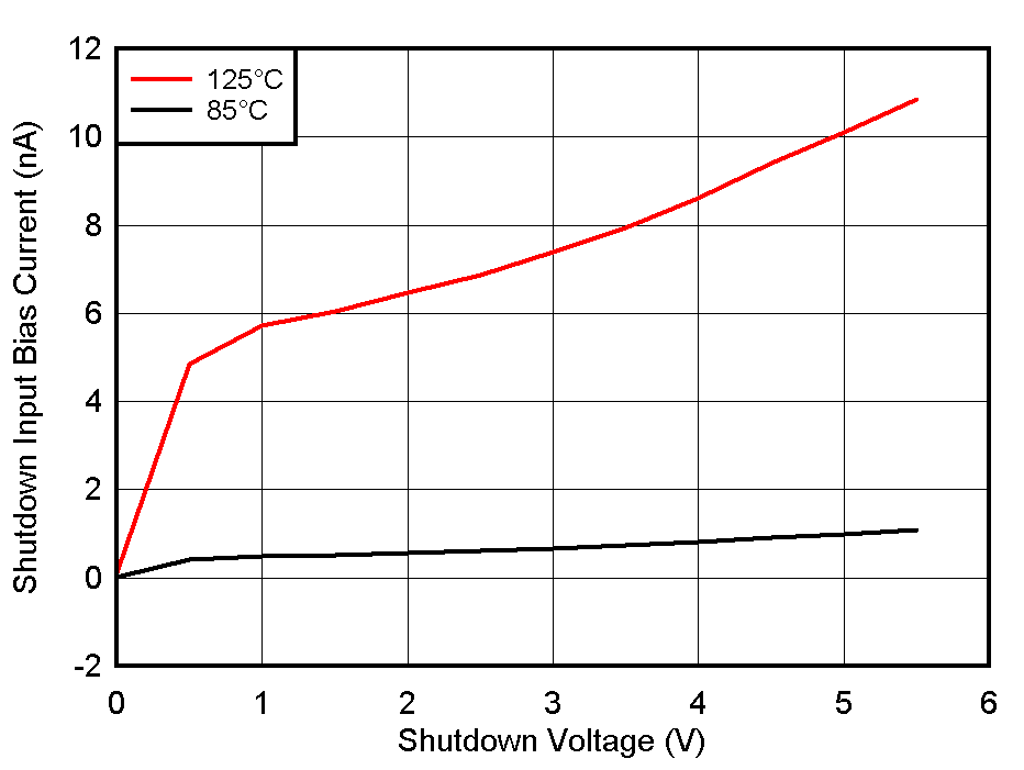
TLV1805-Q1 SDIB_vs_VSD_12V_125_85.gif
Figure 19. Shutdown Input Bias Current vs. Shutdown Input Voltage, High Temperatures
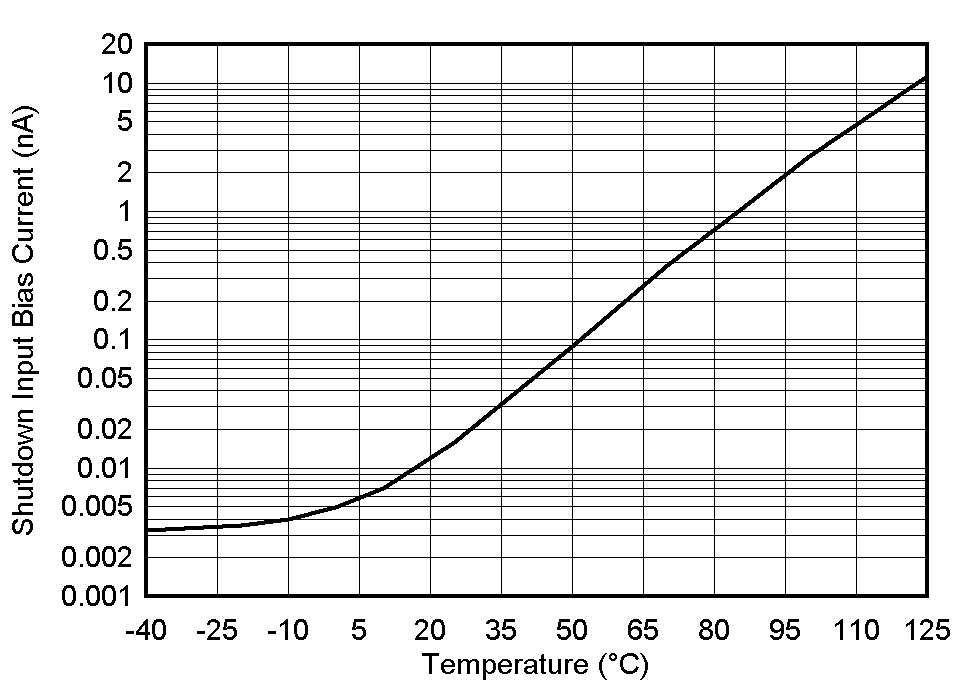
TLV1805-Q1 SDIB_vs_TA.gif
VSD = 5 V
Figure 21. Shutdown Input Bias Current vs. Temperature
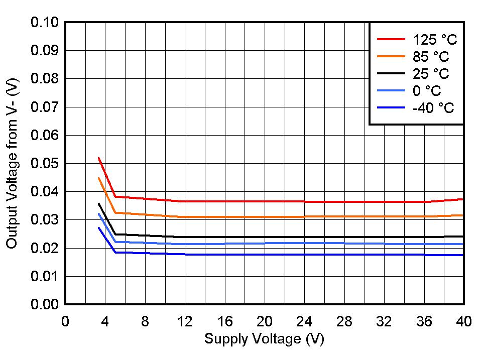
TLV1805-Q1 VOL_vs_Vs.gif
ISINK = 1 mA
Figure 23. Output Low Voltage vs. Supply Voltage
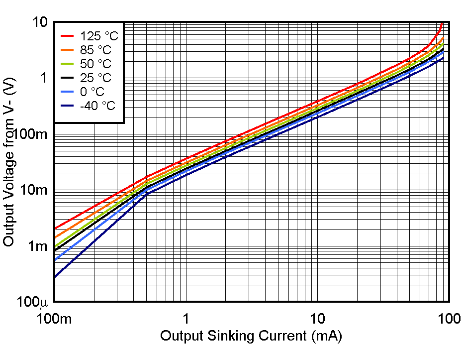
TLV1805-Q1 VOL_vs_IO_Vs3p3.gif
VS = 3.3 V
Figure 25. Output Voltage vs. Output Sinking Current
at 3.3V
TLV1805-Q1 VOL_vs_IO_Vs12.gif
VS = 12 V
Figure 27. Output Voltage vs. Output Sinking Current
at 12V
TLV1805-Q1 VOL_vs_IO_Vs40.gif
VS = 40 V
Figure 29. Output Voltage vs. Output Sinking Current
at 40V
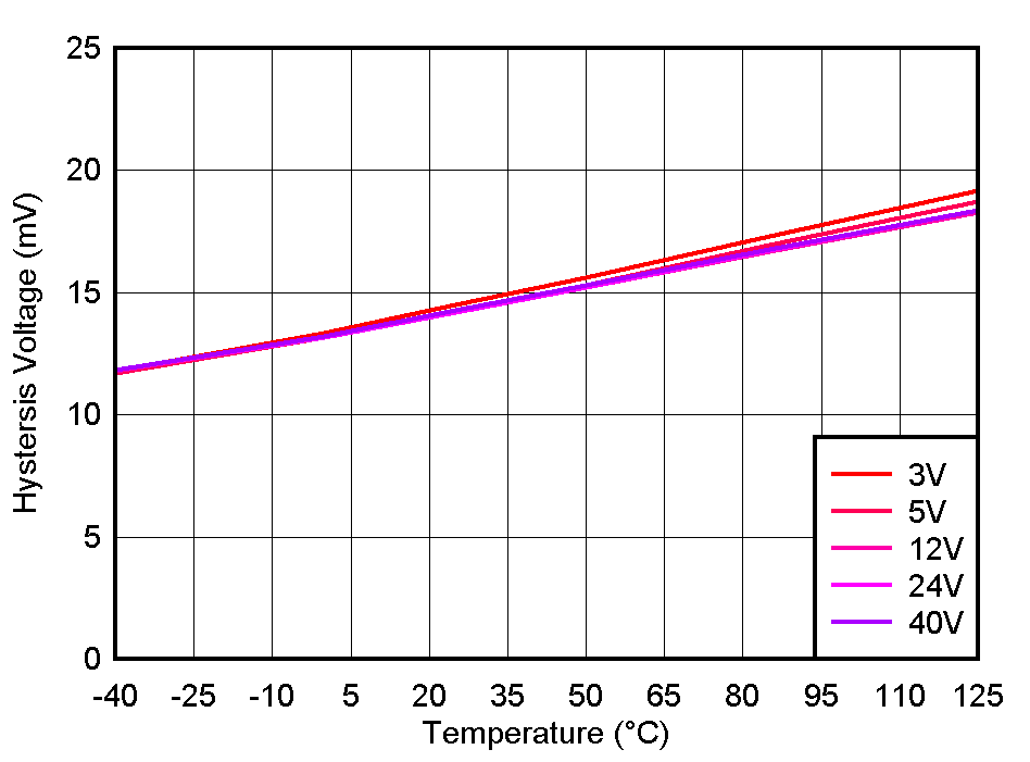
TLV1805-Q1 HYST_vs_TA.gif
Figure 31. Hysteresis vs. Temperature
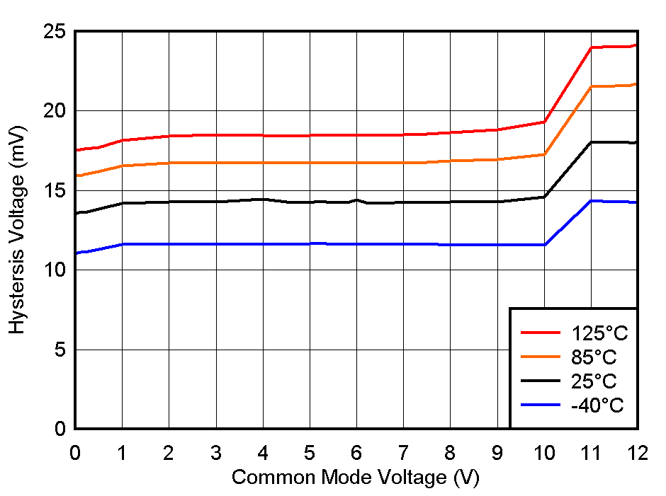
TLV1805-Q1 HYST_vs_VCM.gif
Figure 33. Hysteresis vs Common-Mode Voltage
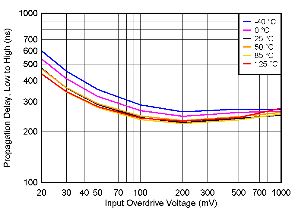
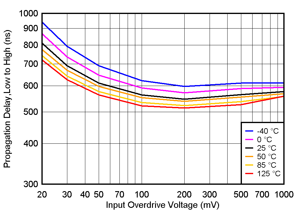
TLV1805-Q1 TPLH_vs_VOD_Vs3p3.gif
VS = 3.3 V CL = 15pF
Figure 35. TPLH Response Time vs. Overdrive
at 3.3V
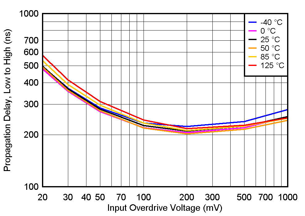
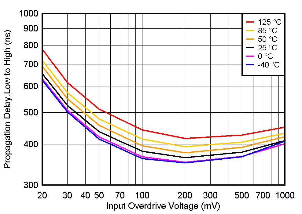
TLV1805-Q1 TPLH_vs_VOD_Vs5.gif
VS = 5 V CL = 15pF
Figure 37. TPLH Response Time vs. Overdrive
at 5V
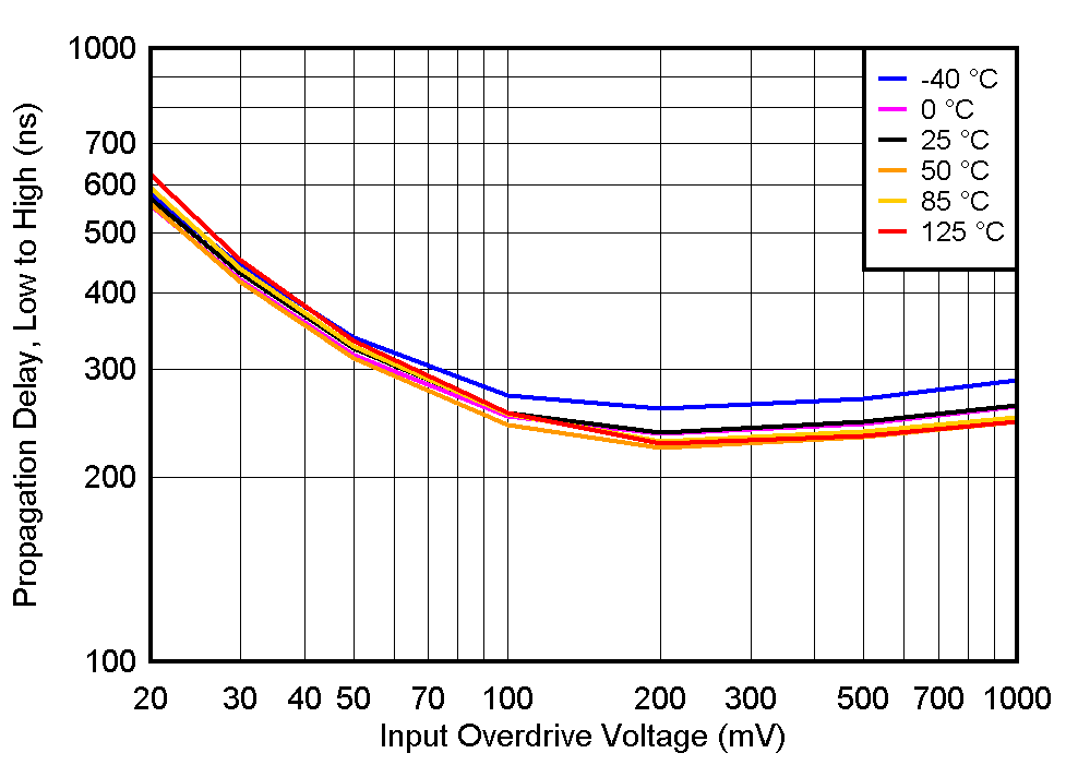
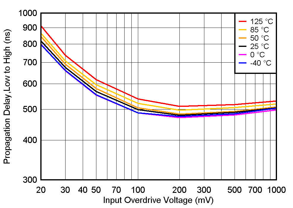
TLV1805-Q1 TPLH_vs_VOD_Vs12.gif
VS = 12 V CL = 15pF
Figure 39. TPLH Response Time vs.
Overdrive at 12V
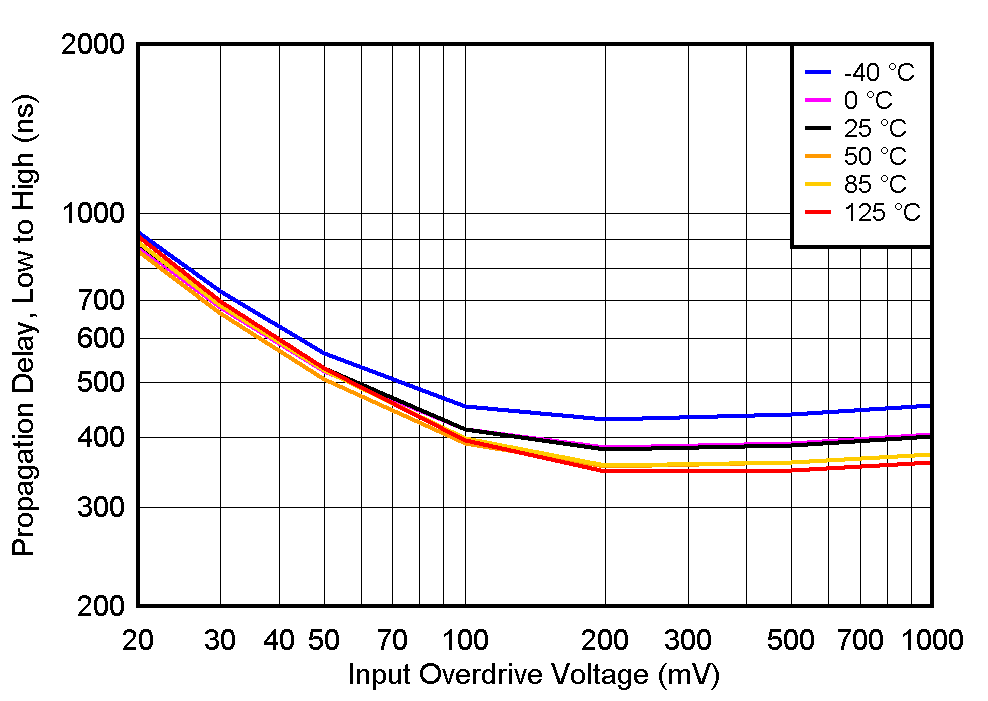
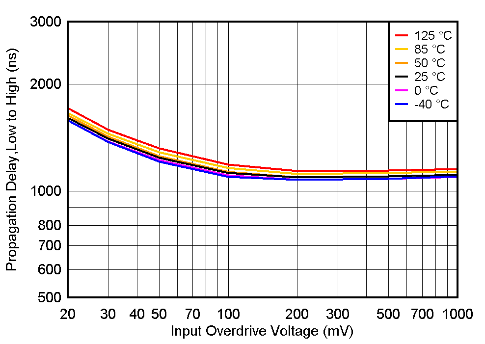
TLV1805-Q1 TPLH_vs_VOD_Vs40.gif
VS = 40 V CL = 15pF
Figure 41. TPLH Response Time vs. Overdrive
at 40V
TLV1805-Q1 TPLH_vs_VOD_Vs3p3_4n.gif
VS = 3.3 V CL = 4nF
Figure 43. TPLH Response Time vs. Overdrive
at 3.3V
TLV1805-Q1 TPLH_vs_VOD_Vs5_4n.gif
VS = 5 V CL = 4nF
Figure 45. TPLH Response Time vs. Overdrive
at 5V
TLV1805-Q1 TPLH_vs_VOD_Vs12_4n.gif
VS = 12 V CL = 4nF
Figure 47. TPLH Response Time vs.
Overdrive at 12V
TLV1805-Q1 TPLH_vs_VOD_Vs40_4n.gif
VS = 40 V CL = 4nF
Figure 49. TPLH Response Time vs. Overdrive
at 40V
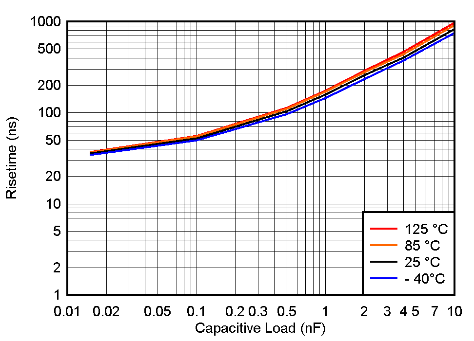
TLV1805-Q1 TR_vs_CL_3p3V.gif
VS = 3.3 V
Figure 51. tRISE vs. Capacitive Load
at 3.3V
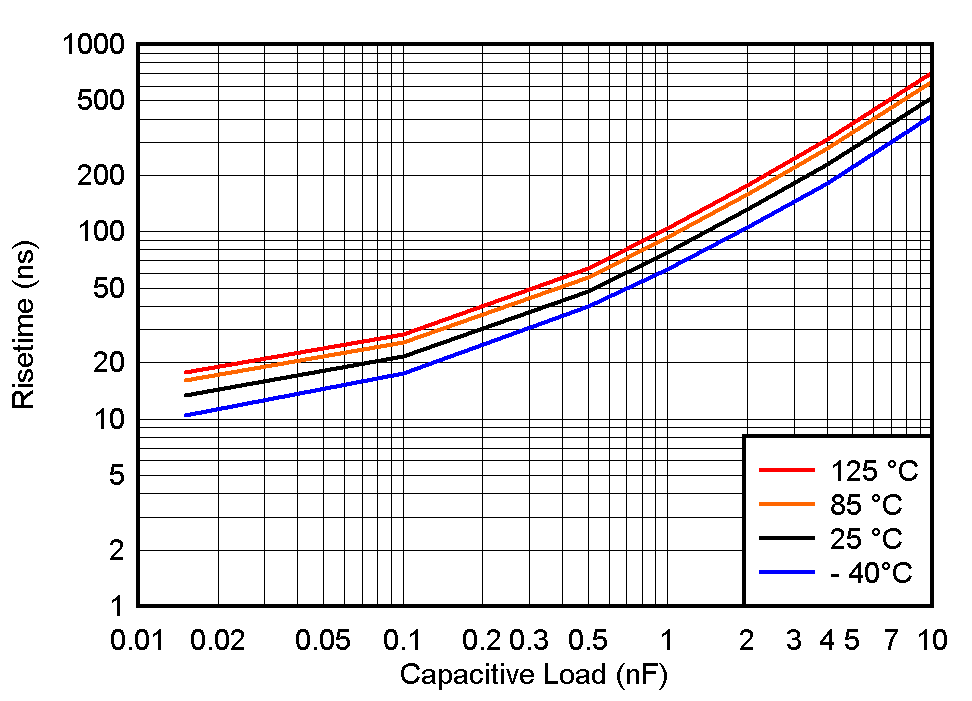
TLV1805-Q1 TR_vs_CL_5V.gif
VS = 5 V
Figure 53. tRISE vs. Capacitive Load
at 5V
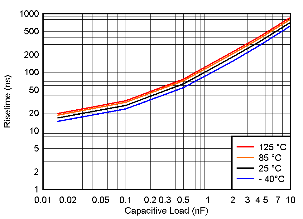
TLV1805-Q1 TR_vs_CL_12V.gif
VS = 12 V
Figure 55. tRISE vs. Capacitive Load
at 12V
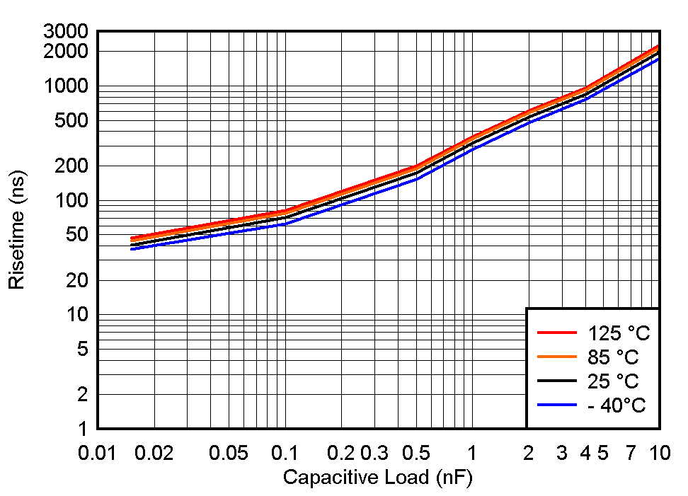
TLV1805-Q1 TR_vs_CL_40V.gif
VS = 40 V
Figure 57. tRISE vs. Capacitive Load
at 40V
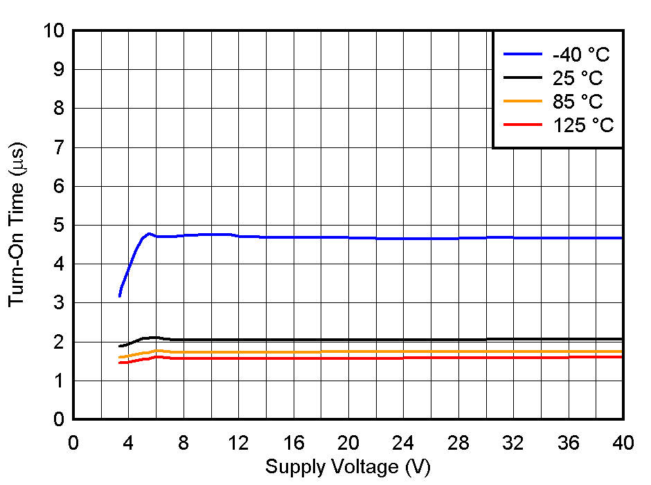
TLV1805-Q1 TON_vs_VS.gif
Figure 59. Turn-On Time vs Supply Voltage
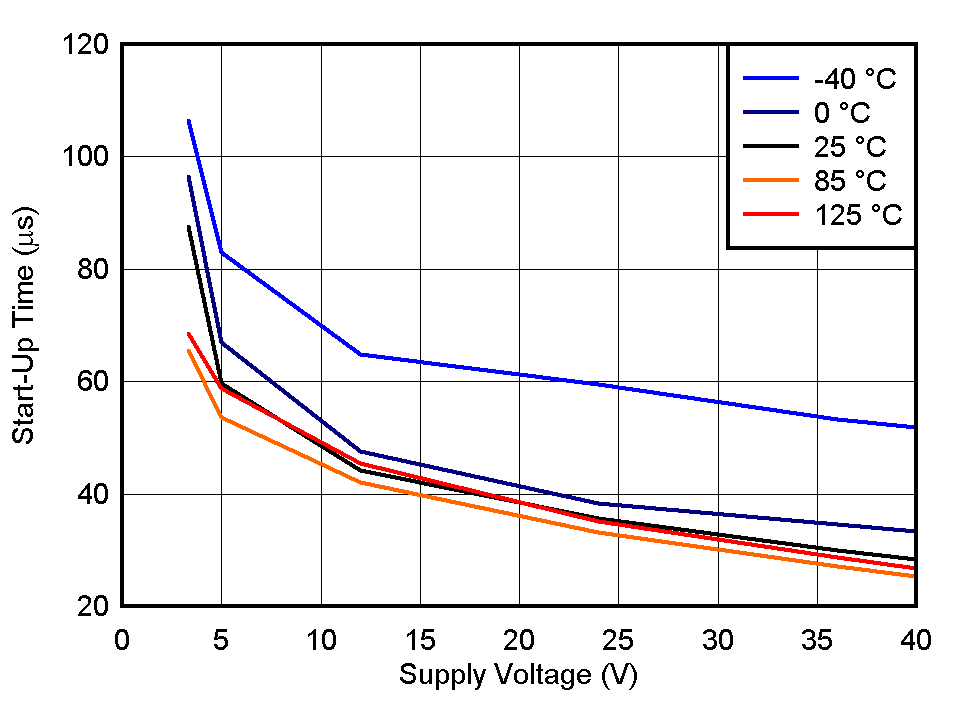
TLV1805-Q1 TSTART_vs_VS.gif
Figure 61. Start-Up Time vs Supply Voltage
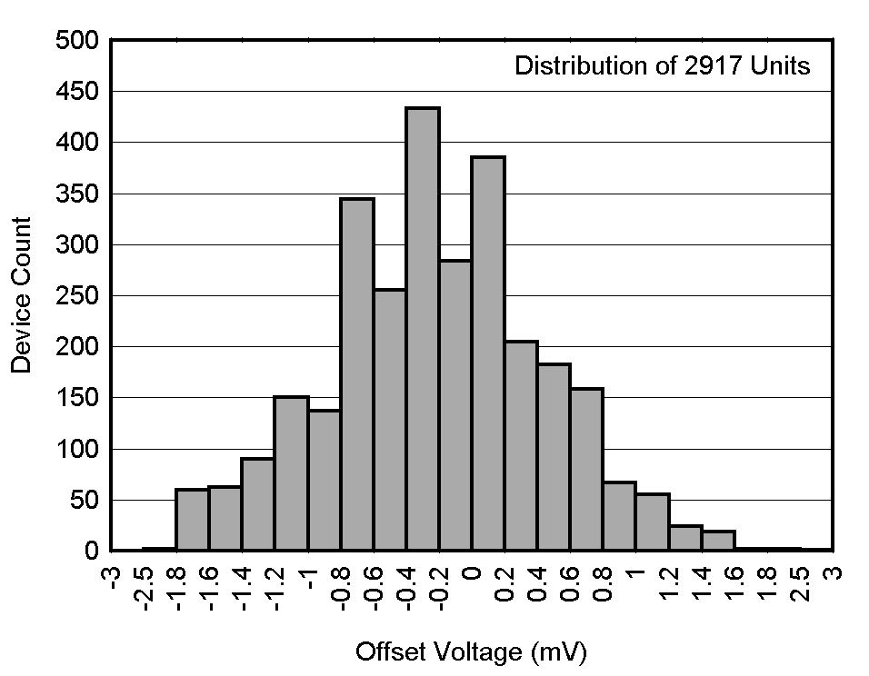
TLV1805-Q1 VIO_HIST.gif
Figure 4. Offset Voltage Histogram
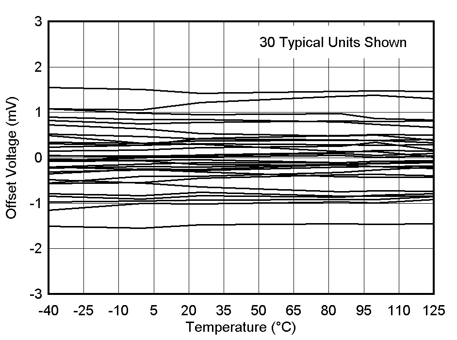
TLV1805-Q1 VIO_vs_TA.gif
Figure 6. Offset Voltage vs Temperature
TLV1805-Q1 IQ_vs_VS_OUTHI.gif
VCM = V- Output High (VID = 0.1 V)
Figure 8. Supply Current vs. Temperature, Output High
TLV1805-Q1 IB_vs_VCM_125C.gif
TA = 125 °C
Figure 10. Input Bias Current vs. Common Mode, 125°C
TLV1805-Q1 IB_vs_VCM_n40C.gif
TA = -40 °C
Figure 12. Input Bias Current vs. Common Mode, -40°C
TLV1805-Q1 IQsd_vs_VS.gif
VCM = V-
Figure 14. Shutdown Supply Current vs. Supply Votlage
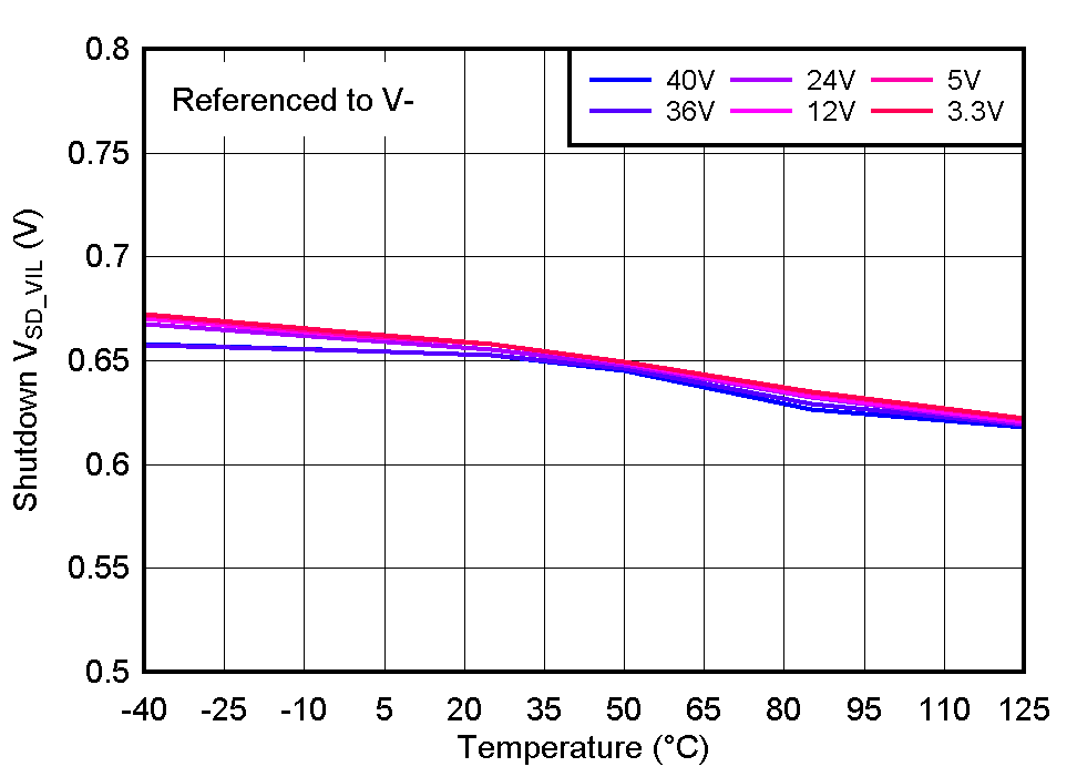
TLV1805-Q1 SDVLO_vs_TA.gif
Figure 16. Shutdown Voltage Low Threshold vs. Temperature
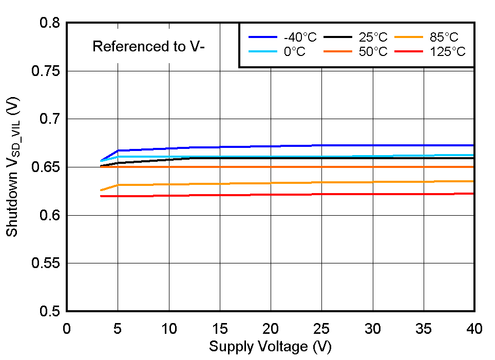
TLV1805-Q1 SDVLO_vs_VS.gif
Figure 18. Shutdown Voltage Low Threshold vs. Supply Voltage
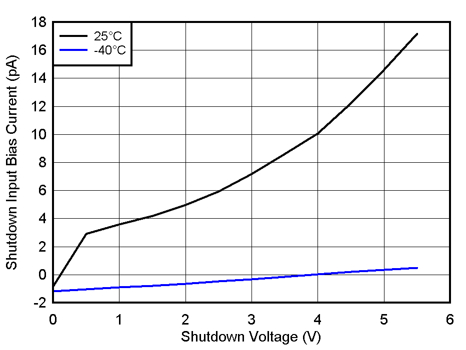
TLV1805-Q1 SDIB_vs_VSD_12V_25_n40.gif
Figure 20. Shutdown Input Bias Current vs. Shutdown Input Voltage, Low Temperatures
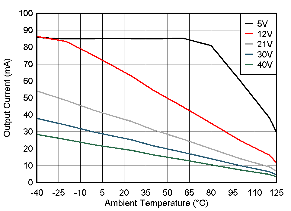
TLV1805-Q1 Detrating.gif
DBV SOT-23-6 Package
Figure 22. Maximum Continuous Output Current vs. Ambient Temperature
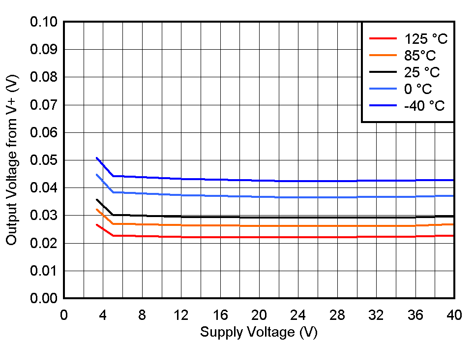
TLV1805-Q1 VOH_vs_Vs.gif
ISOURCE = 1 mA
Figure 24. Output High Voltage vs. Supply Voltage
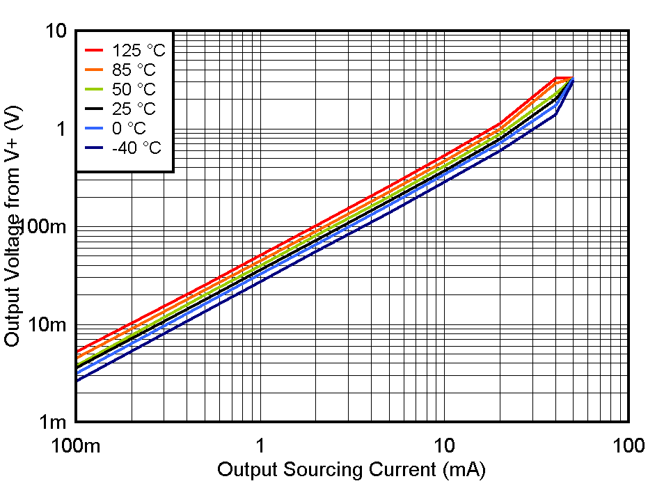
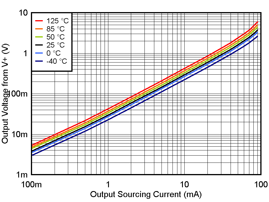
TLV1805-Q1 VOH_vs_IO_Vs3p3.gif
VS = 3.3 V
Figure 26. Output Voltage vs. Output Sourcing Current
at 3.3V
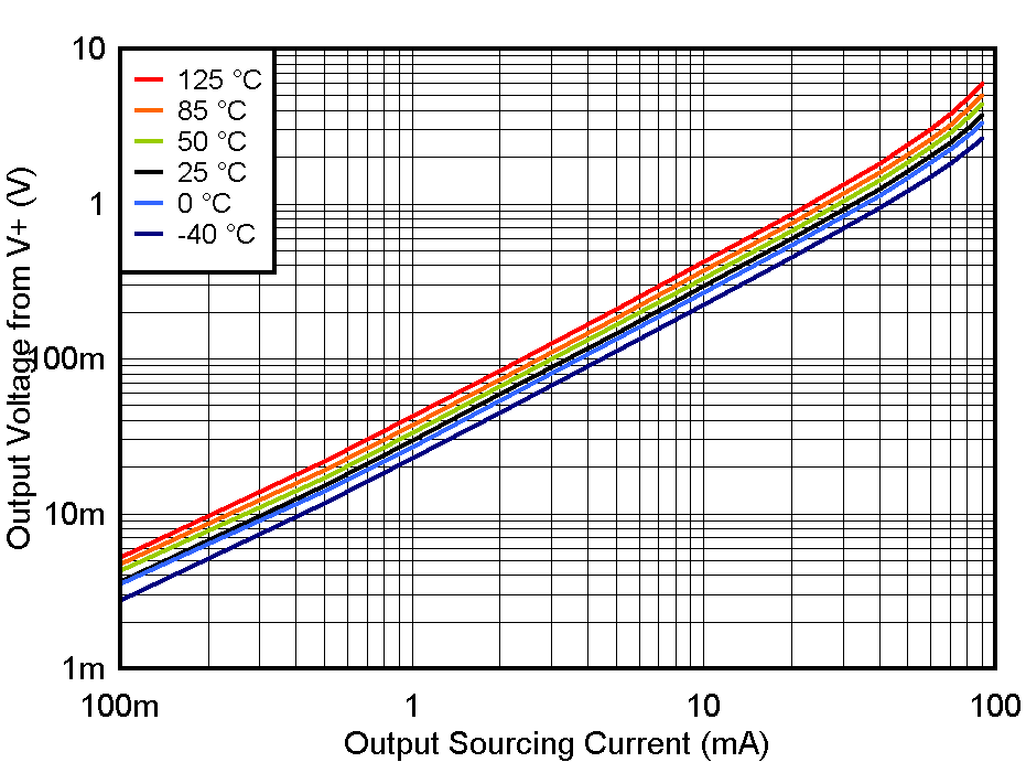
TLV1805-Q1 VOH_vs_IO_Vs12.gif
VS = 12 V
Figure 28. Output Voltage vs. Output Sourcing Current
at 12V
TLV1805-Q1 VOH_vs_IO_Vs40.gif
VS = 40 V
Figure 30. Output Voltage vs. Output Sourcing Current
at 40V
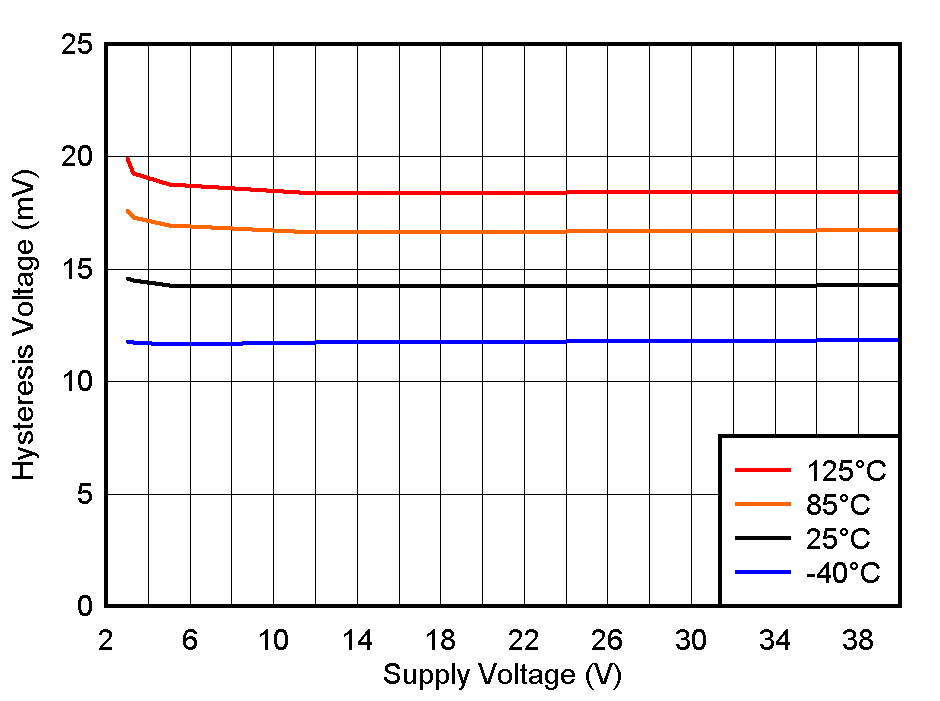
TLV1805-Q1 HYST_vs_VS.gif
Figure 32. Hysteresis vs. Supply Voltage
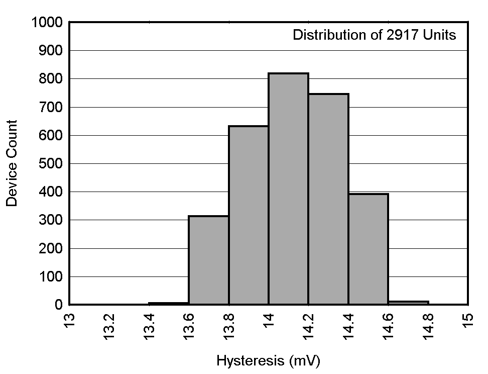
TLV1805-Q1 HYST_HIST.gif
Figure 34. Hysteresis Histogram
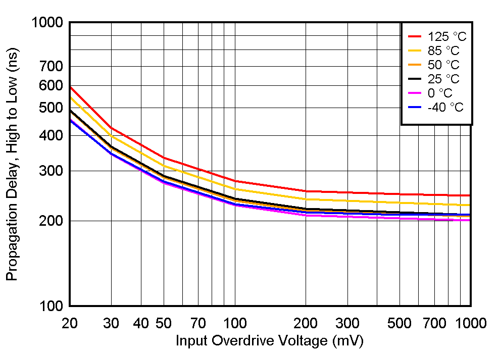
TLV1805-Q1 TPHL_vs_VOD_Vs3p3.gif
VS = 3.3 V CL = 15pF
Figure 36. TPHL Response Time vs. Overdrive
at 3.3V
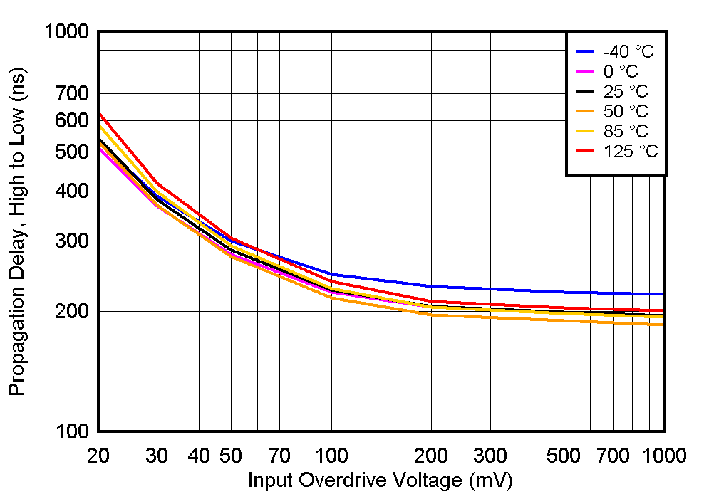
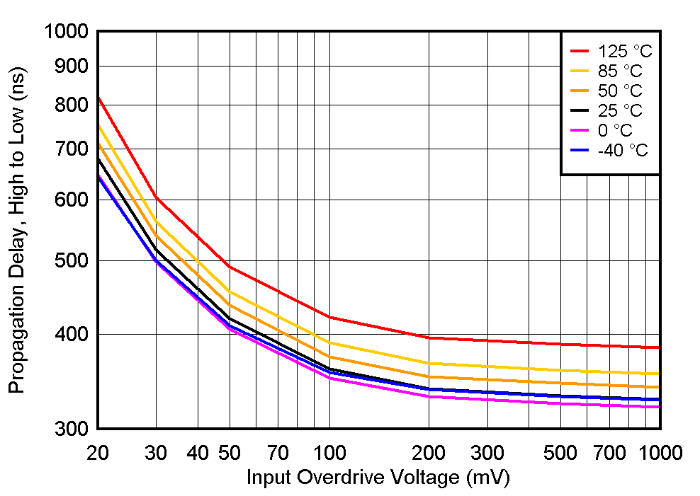
TLV1805-Q1 TPHL_vs_VOD_Vs5.gif
VS = 5 V CL = 15pF
Figure 38. TPHL Response Time vs. Overdrive
at 5V
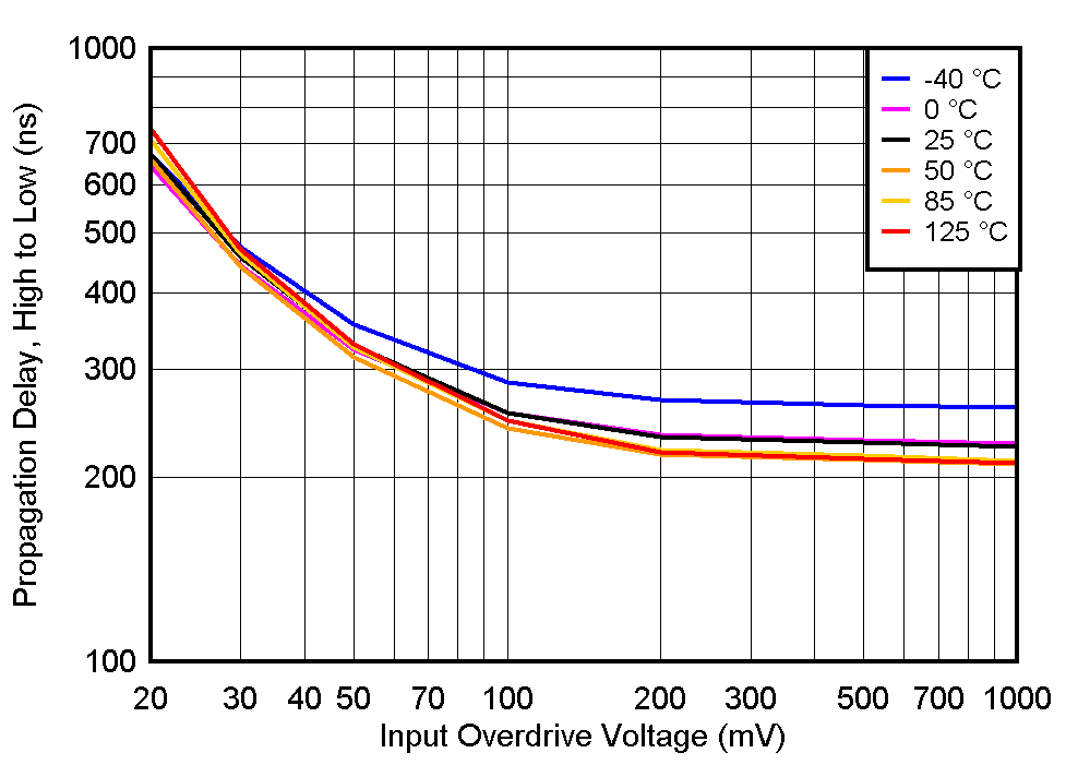
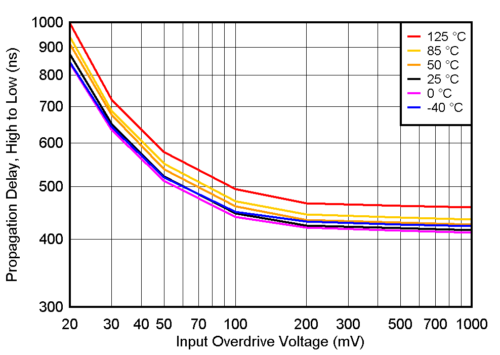
TLV1805-Q1 TPHL_vs_VOD_Vs12.gif
VS = 12 V CL = 15pF
Figure 40. TPHL Response Time vs. Overdrive
at 12V
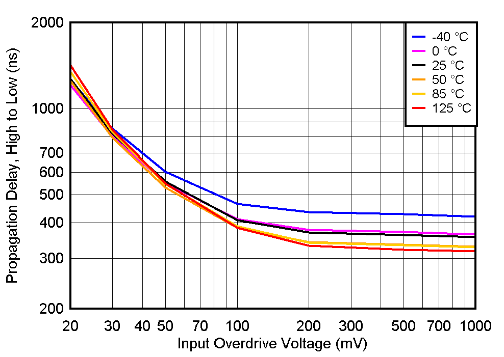
TLV1805-Q1 TPHL_vs_VOD_Vs40.gif
VS = 40 V CL = 15pF
Figure 42. TPHL Response Time vs. Overdrive
at 40V
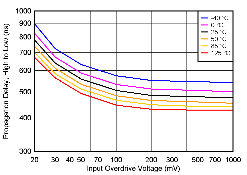
TLV1805-Q1 TPHL_vs_VOD_Vs3p3_4n.gif
VS = 3.3 V CL = 4nF
Figure 44. TPHL Response Time vs. Overdrive
at 3.3V
TLV1805-Q1 TPHL_vs_VOD_Vs5_4n.gif
VS = 5 V CL = 4nF
Figure 46. TPHL Response Time vs. Overdrive
at 5V
TLV1805-Q1 TPHL_vs_VOD_Vs12_4n.gif
VS = 12 V CL = 4nF
Figure 48. TPHL Response Time vs. Overdrive
at 12V
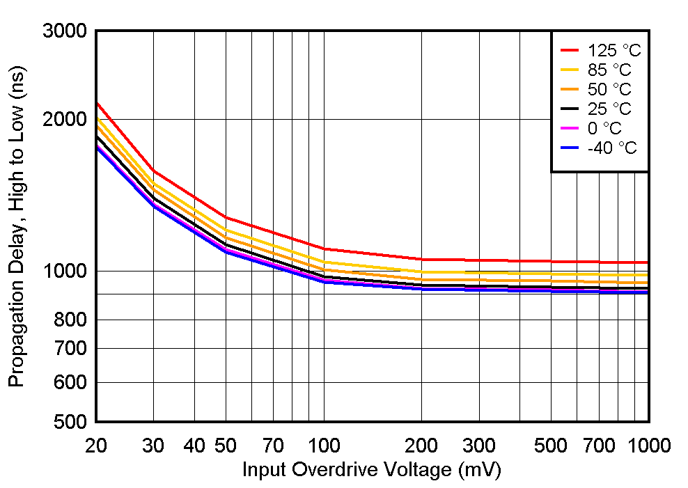
TLV1805-Q1 TPHL_vs_VOD_Vs40_4n.gif
VS = 40 V CL = 4nF
Figure 50. TPHL Response Time vs. Overdrive
at 40V
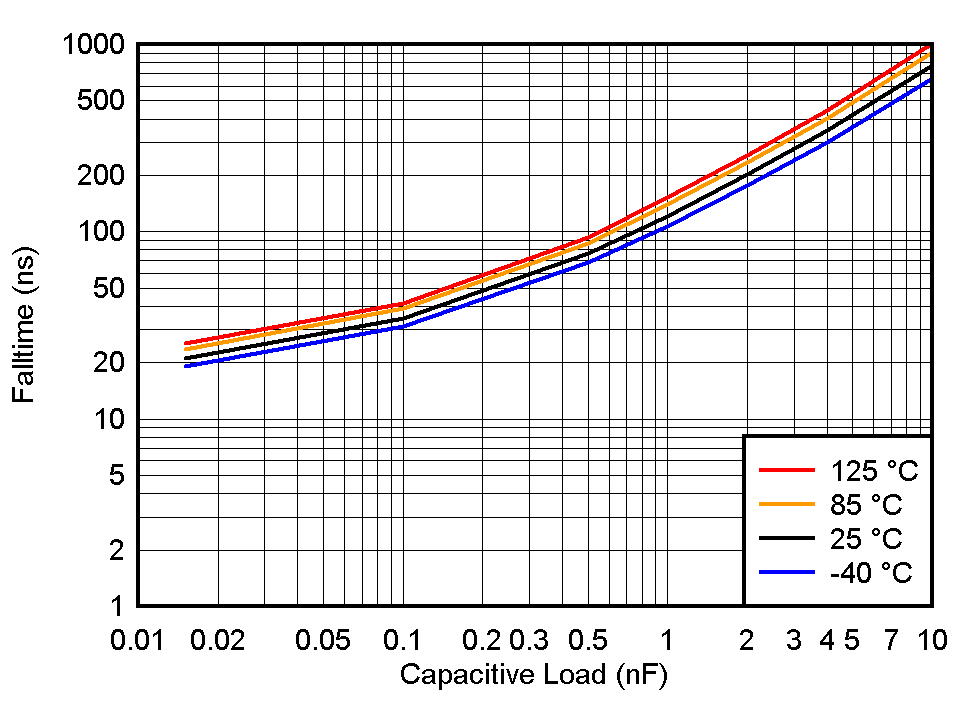
TLV1805-Q1 TF_vs_CL_3p3V.gif
VS = 3.3 V
Figure 52. tFALL vs. Capacitive Load
at 3.3V
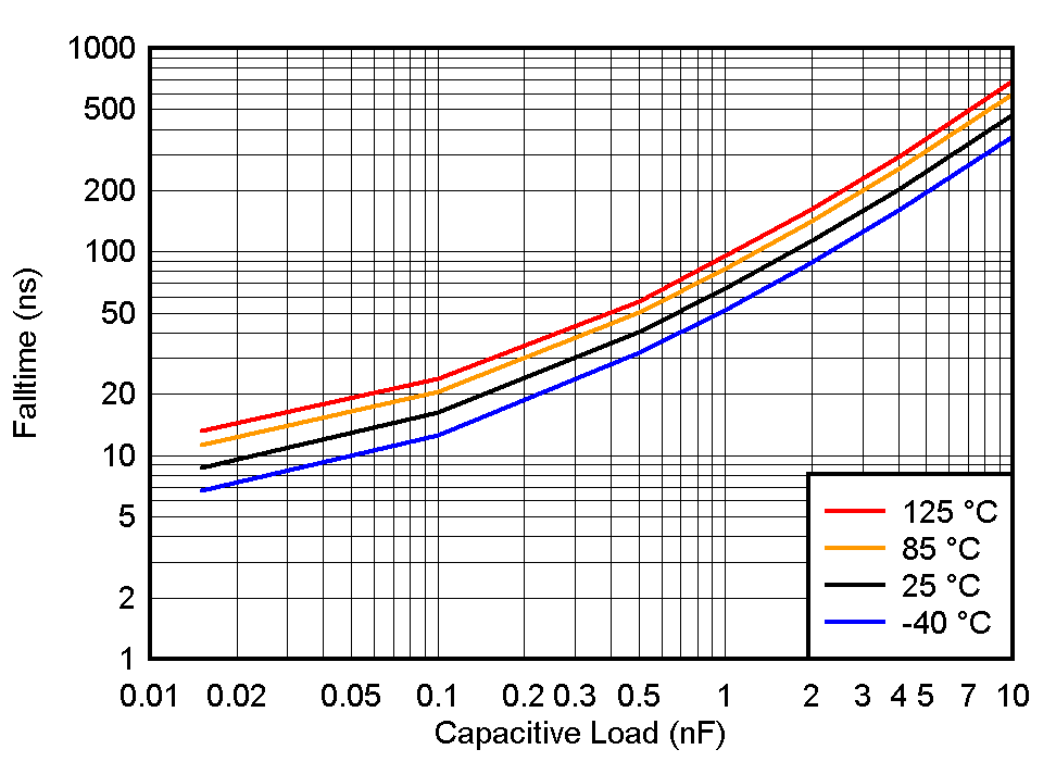
TLV1805-Q1 TF_vs_CL_5V.gif
VS = 5 V
Figure 54. tFALL vs. Capacitive Load
at 5V
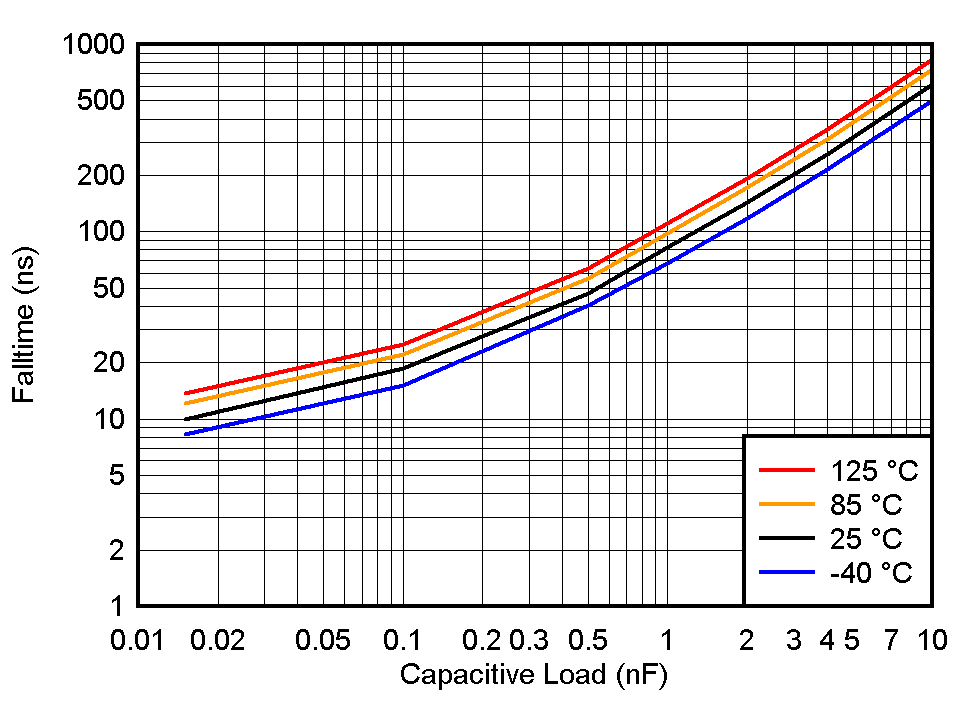
TLV1805-Q1 TF_vs_CL_12V.gif
VS = 12 V
Figure 56. tFALL vs. Capacitive Load
at 12V
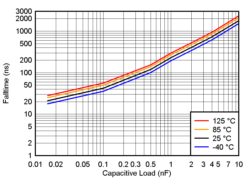
TLV1805-Q1 TF_vs_CL_40V.gif
VS = 40 V
Figure 58. tFALL vs. Capacitive Load
at 40V
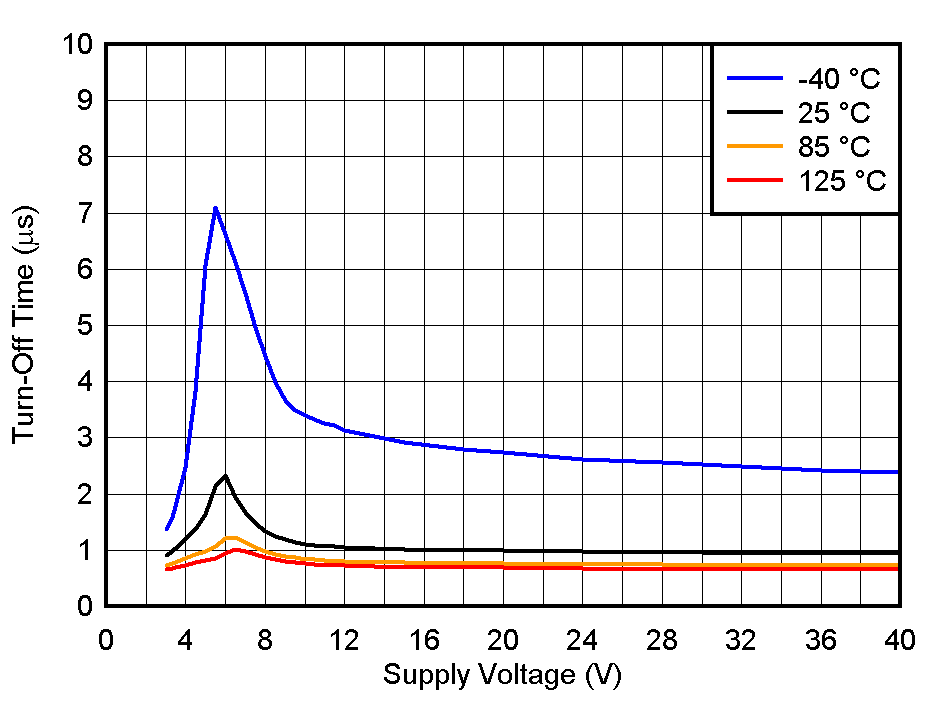
TLV1805-Q1 TOFF_vs_VS.gif
Figure 60. Turn-Off Time vs Supply Voltage
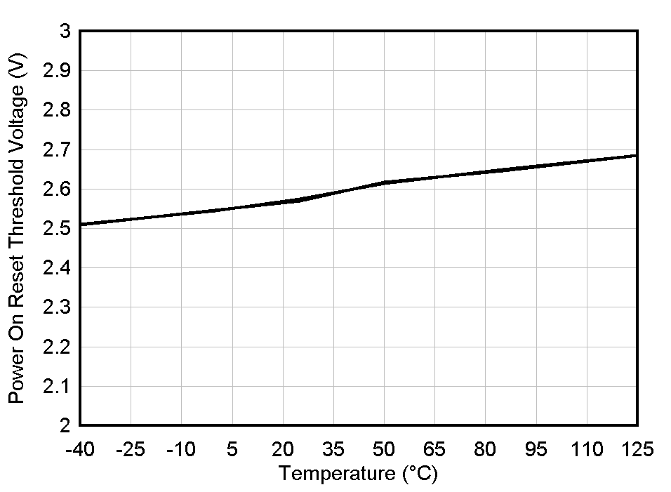
TLV1805-Q1 POR_vs_TA.gif
Figure 62. Power On Reset Voltage vs. Temperature