JAJSGX9B August 2018 – January 2020 TLV1805-Q1
PRODUCTION DATA.
- 1 特長
- 2 アプリケーション
- 3 概要
- 4 改訂履歴
- 5 Pin Configuration and Functions
- 6 Specifications
- 7 Detailed Description
-
8 Application and Implementation
- 8.1 Application Information
- 8.2 Typical Applications
- 9 Power Supply Recommendations
- 10Layout
- 11デバイスおよびドキュメントのサポート
- 12メカニカル、パッケージ、および注文情報
8.2.5 P-Channel Reverse Current Protection Circuit
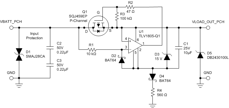
Figure 70 shows the P-Channel circuit. In order to turn "on" the P-Channel MOSFET, the gate must be brought "Low" below VBATT . To accomplish this, the comparators Inverting input is tied to the battery side of the MOSFET to set the output low during forward current.
 Figure 70. P-Channel Reverse Current Schematic
 This design implements a "floating ground" topology, using D3, D4 and R12, to allow for clamping the comparator supply voltage as to not exceed the VGS(MAX) of the MOSFET. During a reverse voltage or supply drop, D4 also prevents C1 from discharging to allow some standby time to keep the comparator powered during the event.
During "normal" forward current operation, the quiescent current of the comparator circuit flows through D4 and R4. D3 provides the clamping during an overvoltage event.
R4 is sized to allow for minimum voltage drop during "normal" operation, but also to allow for dissipation during overvoltage events. R4 will see the battery voltage minus the D3 Zener voltage during an overvoltage event. Since the comparator supply voltage is clamped by D3, the maximum battery voltage is determined by the power dissipated by R4 and the VDS(MAX) of the MOSFET.
R2 limits the gate current should there be any transients and should be a low value to allow the peak currents needed to drive the MOSFET gate capacitance. R3 provides the pull-down needed when the comparator output goes high-Z during power-off to ensure the gate is pulled to zero volts to turn off the MOSFET.
R1 and D2 clamp the input voltage should the VBATT input go below the floating ground Voltage (such as in a battery reversal). A bonus feature is that during a reverse battery voltage condition, D2 and R1 pull the floating ground down towards the negative potential, providing power to the comparator during reverse voltage.
The output clamp diode D5 is used to anchor the output during light or floating loads. At light or no loads, there is a possibility the MOSFET could turn on due to the comparator offset voltage. The diode provides enough of a negative leakage to turn the MOSFET off.
If shutdown of the comparator circuit is desired, a transistor or MOSFET switch can be placed between the ground end of R4 and ground. The MOSFET will be in body diode mode when the comparator is disabled.