SBOS321E March 2005 – April 2016 TLV3501 , TLV3502
PRODUCTION DATA.
- 1 Features
- 2 Applications
- 3 Description
- 4 Revision History
- 5 Pin Configuration and Functions
- 6 Specifications
- 7 Detailed Description
- 8 Application and Implementation
- 9 Power Supply Recommendations
- 10Layout
- 11Device and Documentation Support
- 12Mechanical, Packaging, and Orderable Information
パッケージ・オプション
メカニカル・データ(パッケージ|ピン)
サーマルパッド・メカニカル・データ
- DCN|8
発注情報
5 Pin Configuration and Functions
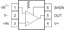
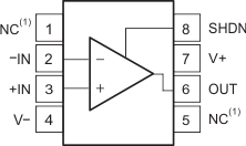
TLV3501: DBV Package1
6-Pin SOT-23
Top View

1. Pin 1 of the 6-pin SOT-23 is determined by orienting the package marking as indicated on the diagram.
Pin Functions: TLV3501
| PIN | I/O | DESCRIPTION | ||
|---|---|---|---|---|
| NAME | SOIC | SOT-23 | ||
| –IN | 2 | 1 | I | Negative (inverting) input |
| +IN | 3 | 3 | I | Positive (noninverting) input |
| NC | 1, 5 | — | — | No internal connection (can be left floating) |
| OUT | 6 | 5 | O | Output |
| SHDN | 8 | 6 | — | Shutdown (the device is idle when this pin is not in use) |
| V– | 4 | 2 | — | Negative (lowest) power supply |
| V+ | 7 | 4 | — | Positive (highest) power supply |
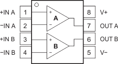
TLV3502: DCN and D Packages
8-Pin SOT-23 and SOIC
Top View

Pin Functions: TLV3502
| PIN | I/O | DESCRIPTION | |
|---|---|---|---|
| NAME | NO. | ||
| –IN A | 2 | I | Inverting input, channel A |
| +IN A | 1 | I | Noninverting input, channel A |
| –IN B | 4 | I | Inverting input, channel B |
| +IN B | 3 | I | Noninverting input, channel B |
| OUT A | 7 | O | Output, channel A |
| OUT B | 6 | O | Output, channel B |
| V– | 5 | — | Negative (lowest) power supply |
| V+ | 8 | — | Positive (highest) power supply |
