JAJSG00A
August 2018 – December 2018
PRODUCTION DATA.
1
特長
2
アプリケーション
3
概要
CMRRおよびPSRRと温度との関係
4
改訂履歴
5
Pin Configuration and Functions
Pin Functions: TLV6001-Q1
Pin Functions: TLV6002-Q1
6
Specifications
6.1
Absolute Maximum Ratings
6.2
ESD Ratings
6.3
Recommended Operating Conditions
6.4
Thermal Information: TLV6001-Q1
6.5
Thermal Information: TLV6002-Q1
6.6
Electrical Characteristics: VS = 1.8 V to 5 V (±0.9 V to ±2.75 V)
6.7
Typical Characteristics: Table of Graphs
6.8
Typical Characteristics
7
Detailed Description
7.1
Overview
7.2
Functional Block Diagram
7.3
Feature Description
7.3.1
Operating Voltage
7.3.2
Rail-to-Rail Input
7.3.3
Rail-to-Rail Output
7.3.4
Common-Mode Rejection Ratio (CMRR)
7.3.5
Capacitive Load and Stability
7.3.6
EMI Susceptibility and Input Filtering
7.4
Device Functional Modes
7.5
Input and ESD Protection
8
Application and Implementation
8.1
Application Information
8.2
Typical Application
8.2.1
Design Requirements
8.2.2
Detailed Design Procedure
8.2.3
Application Curve
8.3
System Examples
9
Power Supply Recommendations
10
Layout
10.1
Layout Guidelines
10.2
Layout Example: Single Channel
10.3
Layout Example: Dual Channel
11
デバイスおよびドキュメントのサポート
11.1
ドキュメントのサポート
11.1.1
関連資料
11.2
関連リンク
11.3
ドキュメントの更新通知を受け取る方法
11.4
コミュニティ・リソース
11.5
商標
11.6
静電気放電に関する注意事項
11.7
Glossary
12
メカニカル、パッケージ、および注文情報
パッケージ・オプション
デバイスごとのパッケージ図は、PDF版データシートをご参照ください。
メカニカル・データ(パッケージ|ピン)
D|8
DGK|8
サーマルパッド・メカニカル・データ
発注情報
jajsg00a_oa
jajsg00a_pm
10.3
Layout Example: Dual Channel
Figure 27.
Schematic Representation for
Figure 25
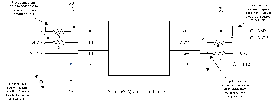
Figure 28.
Layout Example
