JAJSFR4B October   2015  – July 2018 TLV62085

PRODUCTION DATA.  

  1. 1 特長
  2. 2 アプリケーション
  3. 3 概要
    1.     Device Images
      1.      代表的なアプリケーション回路図
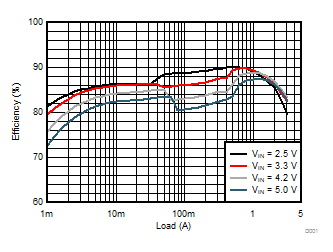
      2.      VIN = 5Vでの効率
  4. 4 改訂履歴
  5. 5 Pin Configuration and Functions
    1.     Pin Functions
  6. 6 Specifications
    1. 6.1 Absolute Maximum Ratings
    2. 6.2 ESD Ratings
    3. 6.3 Recommended Operating Conditions
    4. 6.4 Thermal Information
    5. 6.5 Electrical Characteristics
    6. 6.6 Typical Characteristics
  7. 7 Detailed Description
    1. 7.1 Overview
    2. 7.2 Functional Block Diagram
    3. 7.3 Feature Description
      1. 7.3.1 Power Save Mode
      2. 7.3.2 100% Duty Cycle Low Dropout Operation
      3. 7.3.3 Soft Start
      4. 7.3.4 Switch Current Limit and Hiccup Short-Circuit Protection
      5. 7.3.5 Undervoltage Lockout
      6. 7.3.6 Thermal Shutdown
    4. 7.4 Device Functional Modes
      1. 7.4.1 Enable and Disable
      2. 7.4.2 Power Good
  8. 8 Application and Implementation
    1. 8.1 Application Information
    2. 8.2 Typical Application
      1. 8.2.1 Design Requirements
      2. 8.2.2 Detailed Design Procedure
        1. 8.2.2.1 Custom Design with WEBENCH® Tools
        2. 8.2.2.2 Setting The Output Voltage
        3. 8.2.2.3 Output Filter Design
        4. 8.2.2.4 Inductor Selection
        5. 8.2.2.5 Capacitor Selection
      3. 8.2.3 Application Curves
  9. 9 Power Supply Recommendations
  10. 10Layout
    1. 10.1 Layout Guidelines
    2. 10.2 Layout Example
    3. 10.3 Thermal Considerations
  11. 11デバイスおよびドキュメントのサポート
    1. 11.1 開発サポート
      1. 11.1.1 WEBENCH®ツールによるカスタム設計
      2. 11.1.2 デベロッパー・ネットワークの製品に関する免責事項
    2. 11.2 ドキュメントのサポート
      1. 11.2.1 関連資料
    3. 11.3 ドキュメントの更新通知を受け取る方法
    4. 11.4 コミュニティ・リソース
    5. 11.5 商標
    6. 11.6 静電気放電に関する注意事項
    7. 11.7 Glossary
  12. 12メカニカル、パッケージ、および注文情報

パッケージ・オプション

メカニカル・データ(パッケージ|ピン)
サーマルパッド・メカニカル・データ
発注情報

Application Curves

VIN = 3.6 V, TA = 25 ºC, unless otherwise noted
TLV62085 D001_SLVSD63_TLV62085.gif
VOUT = 0.95 V
Figure 5. Efficiency
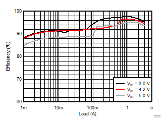
TLV62085 D003_SLVSD63_TLV62085.gif
VOUT = 3.3 V
Figure 7. Efficiency
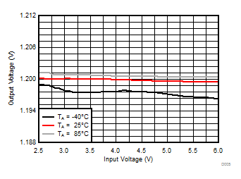
TLV62085 D005_SLVSD63_TLV62085.gif
IOUT = 1 A
Figure 9. Line Regulation
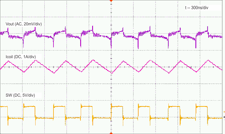
TLV62085 Fig15.gif
IOUT = 3 A VOUT = 1.2 V
Figure 11. PWM Operation
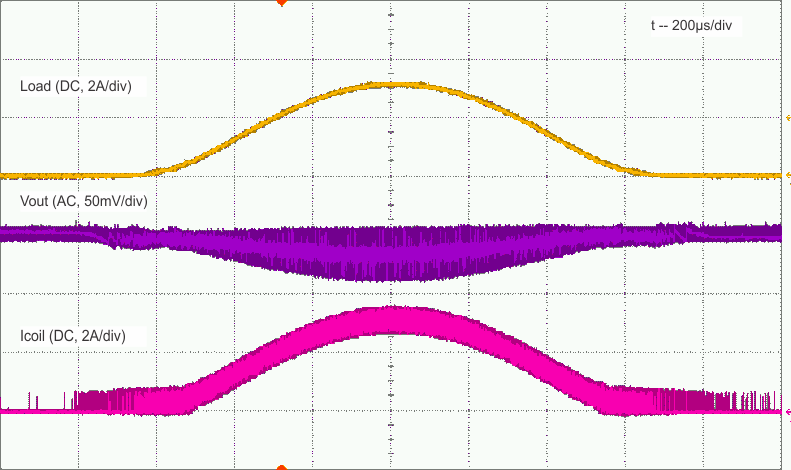
TLV62085 Fig17.gif
IOUT = 0 A to 3 A VOUT = 1.2 V
Figure 13. Load Sweep
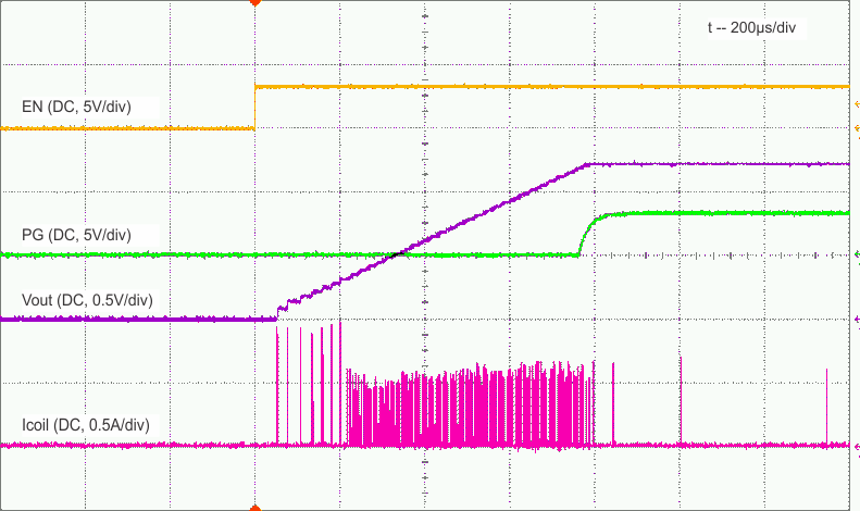
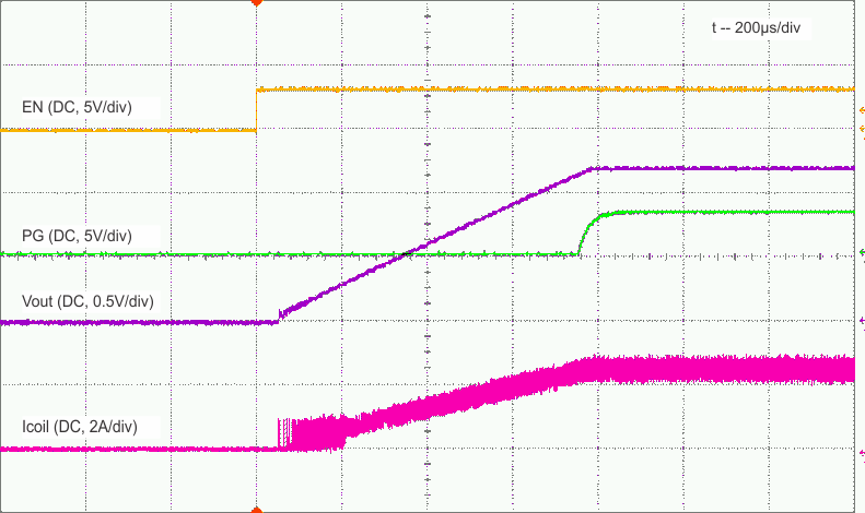
TLV62085 Fig19.gif
VOUT = 1.2 V
Figure 15. Start-Up without Load
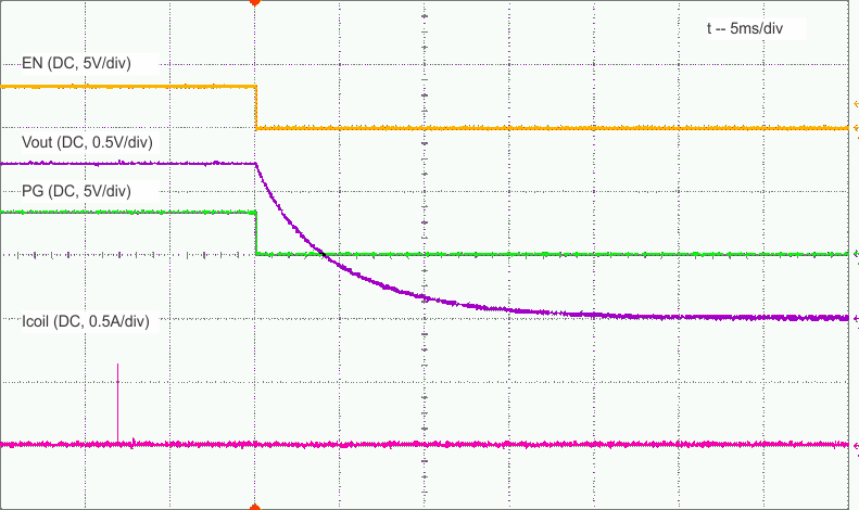
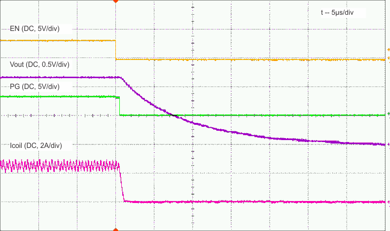
TLV62085 Fig21.gif
VOUT = 1.2 V
Figure 17. Shutdown without Load
TLV62085 Fig23.gif
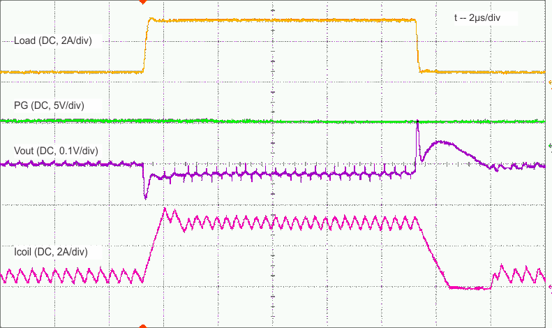
IOUT = 50mA to 3A VOUT = 1.2 V
Figure 19. Load Transient
TLV62085 Fig25.gif
ROUT = 0.47 Ω VOUT = 1.2 V
Figure 21. Output Short-Circuit Protection, Recovery
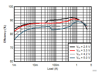
TLV62085 D002_SLVSD63_TLV62085.gif
VOUT = 1.2 V
Figure 6. Efficiency
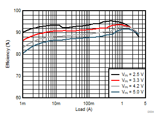
TLV62085 D004_SLVSD63_TLV62085.gif
VOUT = 1.8 V
Figure 8. Efficiency
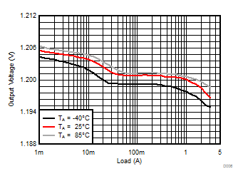
TLV62085 D006_SLVSD63_TLV62085.gif
Figure 10. Load Regulation
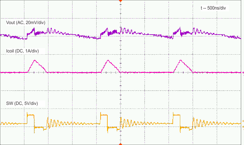
TLV62085 Fig16.gif
IOUT = 0.1 A VOUT = 1.2 V
Figure 12. PFM Operation
TLV62085 Fig18.gif
ROUT = 0.47 Ω VOUT = 1.2 V
Figure 14. Start-Up with Load
TLV62085 Fig20.gif
ROUT = 0.47 Ω VOUT = 1.2 V
Figure 16. Shutdown with Load
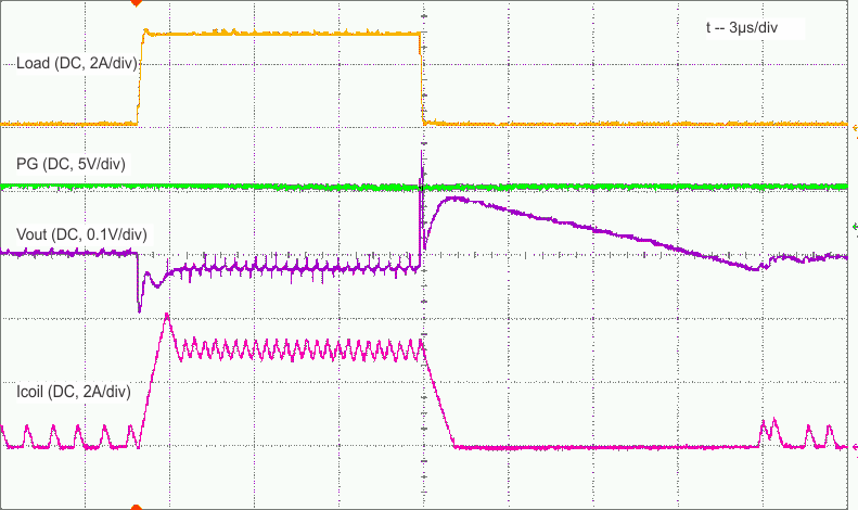
TLV62085 Fig22.gif
IOUT = 0.5 A to 3 A VOUT = 1.2 V
Figure 18. Load Transient
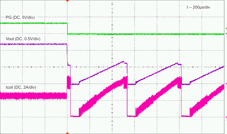
TLV62085 Fig24.gif
ROUT = 0.47 Ω VOUT = 1.2 V
Figure 20. Output Short-Circuit Protection, Entry
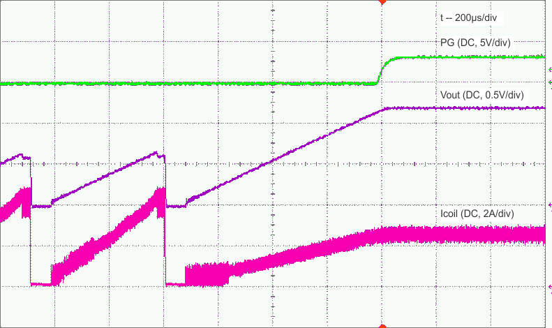
TLV62085 Fig26.gif
ROUT = 0.47 Ω VOUT = 1.2 V
Figure 22. Output Short-Circuit Protection,
HICCUP Zoom In