JAJSKM6 november   2020 TLV6700-Q1

PRODUCTION DATA  

  1.   1
  2. 特長
  3. アプリケーション
  4. 概要
  5. Revision History
  6. Device Comparison Table
  7. Pin Configuration and Functions
  8. Specifications
    1. 7.1 Absolute Maximum Ratings
    2. 7.2 ESD Ratings
    3. 7.3 Recommended Operating Conditions
    4. 7.4 Thermal Information
    5. 7.5 Electrical Characteristics
    6. 7.6 Timing Requirements
    7. 7.7 Switching Characteristics
    8. 7.8 Timing Diagrams
    9. 7.9 Typical Characteristics
  9. Detailed Description
    1. 8.1 Overview
    2. 8.2 Functional Block Diagram
    3. 8.3 Feature Description
      1. 8.3.1 Inputs (INA+, INB–)
      2. 8.3.2 Outputs (OUTA, OUTB)
      3. 8.3.3 Window Comparator
      4. 8.3.4 Immunity to Input Terminal Voltage Transients
    4. 8.4 Device Functional Modes
      1. 8.4.1 Normal Operation (VDD > UVLO)
      2. 8.4.2 Undervoltage Lockout (V(POR) < VDD < UVLO)
      3. 8.4.3 Power-On Reset (VDD < V(POR))
  10. Application and Implementation
    1. 9.1 Application Information
      1. 9.1.1 VPULLUP to a Voltage Other Than VDD
      2. 9.1.2 Monitoring VDD
      3. 9.1.3 Monitoring a Voltage Other Than VDD
    2. 9.2 Typical Application
      1. 9.2.1 Design Requirements
      2. 9.2.2 Detailed Design Procedure
        1. 9.2.2.1 Resistor Divider Selection
        2. 9.2.2.2 Pullup Resistor Selection
        3. 9.2.2.3 Input Supply Capacitor
        4. 9.2.2.4 Input Capacitors
      3. 9.2.3 Application Curves
    3. 9.3 Do's and Don'ts
  11. 10Power Supply Recommendations
  12. 11Layout
    1. 11.1 Layout Guidelines
    2. 11.2 Layout Example
  13. 12Device and Documentation Support
    1. 12.1 Device Support
      1. 12.1.1 Development Support
    2. 12.2 Receiving Notification of Documentation Updates
    3. 12.3 サポート・リソース
    4. 12.4 Trademarks
    5. 12.5 静電気放電に関する注意事項
    6. 12.6 用語集
  14. 13Mechanical, Packaging, and Orderable Information

パッケージ・オプション

メカニカル・データ(パッケージ|ピン)
サーマルパッド・メカニカル・データ
発注情報

Resistor Divider Selection

Use Equation 1 through Equation 4 to calculate the resistor divider values and target threshold voltages.

Equation 1. RT = R1 + R2 + R3

Select a value for RT such that the current through the divider is approximately 100 times higher than the input current at the INA+ and INB– terminals. The resistors can have high values to minimize current consumption as a result of low-input bias current without adding significant error to the resistive divider. See the application note Optimizing Resistor Dividers at a Comparator Input (SLVA450) for details on sizing input resistors.

Use Equation 2 to calculate the value of R3.
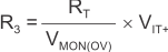
Equation 2. GUID-496CB697-ED9A-4063-8D14-33ED708E36CA-low.gif

where:

VMON(OV) is the target voltage at which an overvoltage condition is detected

Use Equation 3 or Equation 4 to calculate the value of R2.
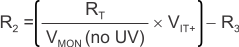
Equation 3. GUID-34E50E7E-08E8-41E5-9ED1-6D9A2DB34E92-low.gif

where:

VMON(no UV) is the target voltage at which an undervoltage condition is removed as VMON rises
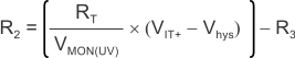
Equation 4. GUID-428E37C0-59C0-4882-AB05-A3627E0AC44A-low.gif

where:

VMON(UV) is the target voltage at which an undervoltage condition is detected

The worst-case tolerance can be calculated by referring to Equation 13 in application report SLVA450, Optimizing Resistor Dividers at a Comparator Input (available for download at www.ti.com). An example of the rising threshold error, VMON(OV), is given in Equation 5.

Equation 5. GUID-E8137F9F-6729-4516-A1C9-BF841D69AE4C-low.gif