JAJSHO5C October 2014 – July 2019 TLV733P
PRODUCTION DATA.
- 1 特長
- 2 アプリケーション
- 3 概要
- 4 改訂履歴
- 5 Pin Configuration and Functions
- 6 Specifications
- 7 Detailed Description
- 8 Application and Implementation
- 9 Power Supply Recommendations
- 10Layout
- 11デバイスおよびドキュメントのサポート
- 12メカニカル、パッケージ、および注文情報
パッケージ・オプション
デバイスごとのパッケージ図は、PDF版データシートをご参照ください。
メカニカル・データ(パッケージ|ピン)
- DBV|5
- DQN|4
サーマルパッド・メカニカル・データ
発注情報
8.1.1 Input and Output Capacitor Selection
The TLV733 uses an advanced internal control loop to obtain stable operation both with and without the use of input or output capacitors. Dynamic performance is improved with the use of an output capacitor, and may be improved with an input capacitor. An output capacitance of 0.1 μF or larger generally provides good dynamic response. Use X5R- and X7R-type ceramic capacitors because these capacitors have minimal variation in value and equivalent series resistance (ESR) over temperature.
Although an input capacitor is not required for stability, increased output impedance from the input supply may compromise the performance of the TLV733. Good analog design practice is to connect a 0.1-µF to 1-µF capacitor from IN to GND. This capacitor counteracts reactive input sources and improves transient response, input ripple, and PSRR. Use an input capacitor if the source impedance is greater than 0.5 Ω. Use a higher-value capacitor if large, fast, rise-time load transients are anticipated, or if the device is located several inches from the input power source.
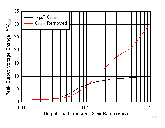
Figure 33 shows the transient performance improvements with an external 1-µF capacitor on the output versus no output capacitor. The data in this figure are taken with an increasing load step from 50 mA to 300 mA, and the peak output voltage deviation (load transient response) is measured. For low output current slew rates,
(< 0.1 A/µs), the transient performance of the device is similar with or without an output capacitor. As the current slew rate is increased, the peak voltage deviation is significantly increased. For loads that exhibit fast current slew rates above 0.1 A/µs, use an output capacitor. For best performance, the maximum recommended output capacitance is 100 µF.

| TLV73333PDBV, output current stepped from 50 mA to 300 mA, output voltage change measured at positive dI/dt |
Some applications benefit from the removal of the output capacitor. In addition to space and cost savings, the removal of the output capacitor lowers inrush current as a result of eliminating the required current flow into the output capacitor upon startup. In these cases, take care to ensure that the load is tolerant of the additional output voltage deviations.