JAJSE96C October 2017 – March 2024 TLV757P
PRODUCTION DATA
- 1
- 1 特長
- 2 アプリケーション
- 3 概要
- 4 Pin Configuration and Functions
- 5 Specifications
- 6 Detailed Description
- 7 Application and Implementation
- 8 Device and Documentation Support
- 9 Revision History
- 10Mechanical, Packaging, and Orderable Information
パッケージ・オプション
デバイスごとのパッケージ図は、PDF版データシートをご参照ください。
メカニカル・データ(パッケージ|ピン)
- DYD|5
- DBV|5
- DRV|6
サーマルパッド・メカニカル・データ
- DRV|6
発注情報
6.3.2 Enable (EN)
The enable pin (EN) is active high. Enable the device by forcing the EN pin to exceed VHI. Turn off the device by forcing the EN pin below VLO. If shutdown capability is not required, connect EN to IN.
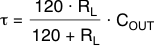
The device has an internal pull-down that connects a 120Ω resistor to ground when the device is disabled. The discharge time after disabling depends on the output capacitance (COUT) and the load resistance (RL) in parallel with the 120Ω pulldown resistor. Equation 1 calculates the time constant τ:
The EN pin is independent of the input pin. However, if the EN pin is driven to a higher voltage than VIN, the current into the EN pin increases. This effect is illustrated in Figure 5-24. When the EN voltage is higher than the input voltage there is an increased current flow into the EN pin. If this increased flow causes problems in the application, sequence the EN pin after VIN is high, or tie EN to VIN. If EN is driven to a higher voltage than VIN, limit the frequency on EN to below 10kHz.