JAJSDY7A June   2017  – October 2017 TLV760

PRODUCTION DATA.  

  1. 特長
  2. アプリケーション
  3. 概要
  4. 改訂履歴
  5. Pin Configuration and Functions
  6. Specifications
    1. 6.1 Absolute Maximum Ratings
    2. 6.2 ESD Ratings
    3. 6.3 Recommended Operating Conditions
    4. 6.4 Thermal Information
    5. 6.5 Electrical Characteristics
    6. 6.6 Typical Characteristics
  7. Detailed Description
    1. 7.1 Overview
    2. 7.2 Functional Block Diagram
    3. 7.3 Feature Description
      1. 7.3.1 Thermal Protection
      2. 7.3.2 Dropout Voltage
    4. 7.4 Device Functional Modes
      1. 7.4.1 Normal Operation
  8. Application and Implementation
    1. 8.1 Application Information
      1. 8.1.1 Fixed Output
      2. 8.1.2 External Capacitors
        1. 8.1.2.1 Input and Output Capacitor Requirements
        2. 8.1.2.2 Load-Step Transient Response
      3. 8.1.3 Power Dissipation
    2. 8.2 Typical Application
      1. 8.2.1 Design Requirements
      2. 8.2.2 Detailed Design Procedure
      3. 8.2.3 Application Curves
  9. Power Supply Recommendations
  10. 10Layout
    1. 10.1 Layout Guidelines
    2. 10.2 Layout Example
  11. 11デバイスおよびドキュメントのサポート
    1. 11.1 デバイス・サポート
      1. 11.1.1 関連資料
      2. 11.1.2 SPICEモデル
      3. 11.1.3 デバイスの項目表記
    2. 11.2 ドキュメントの更新通知を受け取る方法
    3. 11.3 コミュニティ・リソース
    4. 11.4 商標
    5. 11.5 静電気放電に関する注意事項
    6. 11.6 Glossary
  12. 12メカニカル、パッケージ、および注文情報

パッケージ・オプション

メカニカル・データ(パッケージ|ピン)
サーマルパッド・メカニカル・データ
発注情報

Pin Configuration and Functions

DBZ Package
3-Pin SOT-23
Top View
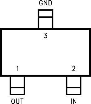
TLV760 10007001.png

Pin Functions

PIN I/O DESCRIPTION
NO. NAME
1 OUT O Output voltage, a ceramic capacitor greater than or equal to 0.1 μF is need for the stability of the device.(1)
2 IN I Input voltage supply — TI recommends a capacitor of value greater than 0.1 µF at the input.(1)
3 GND Common ground
See External Capacitors for more details.