SLASE75D August 2015 – September 2017 TMDS181
PRODUCTION DATA.
- 1 Features
- 2 Applications
- 3 Description
- 4 Revision History
- 5 Pin Configuration and Functions
-
6 Specifications
- 6.1 Absolute Maximum Ratings
- 6.2 ESD Ratings
- 6.3 Recommended Operating Conditions
- 6.4 Thermal Information
- 6.5 Power Supply Electrical Characteristics
- 6.6 TMDS Differential Input Electrical Characteristics
- 6.7 TMDS Differential Output Electrical Characteristics
- 6.8 DDC, I2C, HPD, and ARC Electrical Characteristics
- 6.9 Power-Up and Operation Timing Requirements
- 6.10 TMDS Switching Characteristics
- 6.11 HPD Switching Characteristics
- 6.12 DDC and I2C Switching Characteristics
- 6.13 Typical Characteristics
- 7 Parameter Measurement Information
-
8 Detailed Description
- 8.1 Overview
- 8.2 Functional Block Diagram
- 8.3
Feature Description
- 8.3.1 Reset Implementation
- 8.3.2 Operation Timing
- 8.3.3 Swap and Polarity Working
- 8.3.4 TMDS Inputs
- 8.3.5 TMDS Inputs Debug Tools
- 8.3.6 Receiver Equalizer
- 8.3.7 Input Signal Detect Block
- 8.3.8 Audio Return Channel
- 8.3.9 Transmitter Impedance Control
- 8.3.10 TMDS Outputs
- 8.3.11 Pre-Emphasis/De-Emphasis
- 8.4 Device Functional Modes
- 8.5 Register Maps
- 9 Application and Implementation
- 10Power Supply Recommendations
- 11Layout
- 12Device and Documentation Support
- 13Mechanical, Packaging, and Orderable Information
パッケージ・オプション
メカニカル・データ(パッケージ|ピン)
- RGZ|48
サーマルパッド・メカニカル・データ
- RGZ|48
発注情報
9 Application and Implementation
NOTE
Information in the following applications sections is not part of the TI component specification, and TI does not warrant its accuracy or completeness. TI’s customers are responsible for determining suitability of components for their purposes. Customers should validate and test their design implementation to confirm system functionality.
9.1 Application Information
The TMDS181 was defined to work in many applications. This includes source applications like a Blu-ray™ DVD player or AVR. The adaptive receive equalizer makes it ideal for sink applications like UHDTV, monitors, and projectors where cable length can be widely varied. When in a sink application, the designer must consider several system-level architectures. The TMDS181 is also capable of working in an active cable to extend the cable length even further.
9.2 Typical Applications
9.2.1 Source Side Application
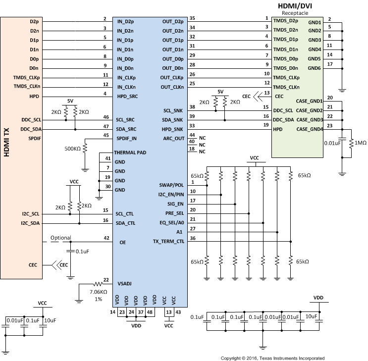 Figure 32. TMDS181 in Source Side Application
9.2.1.1 Design Requirements
The TMDS181 can be designed into many different applications. All applications have certain requirements for the system to work properly. Two voltage rails are required to support the lowest power consumption possible. The OE pin must have a 0.1 µF capacitor to ground. This pin can be driven by a processor, but the pin needs to change states after voltage rails have stabilized. The best way to configure the device is by using I2C. However, pin strapping is provided because I2C is not available in all cases. As sources may have different naming conventions, it is necessary to confirm that the link between the source and the TMDS181 are correctly mapped. A swap function is provide for the input pins in case signaling is reversed between source and device. The control pin values in Table 9 are based upon driving pins with a microcontroller; otherwise, the shown pullup/pulldown configuration meet device levels. Table 9 provides information on expected values in order to perform properly.
Table 9. Design Parameters
| DESIGN PARAMETER | VALUE |
|---|---|
| VCC | 3.3 V |
| VDD | 1.2 V |
| Main link input voltage | VID = 75 mVpp to 1.2 Vpp |
| Control pin max voltage for low | 65 kΩ resistor connected to GND |
| Control pin voltage range mid | Not connected |
| Control pin min voltage for high | 65 kΩ resistor connected to Vcc |
| VSADJ resistor | 7.06 kΩ 1% |
9.2.1.2 Detailed Design Procedure
The TMDS181 is a signal conditioning device that provides several forms of signal conditioning to support compliance for HDMI or DVI at a source connector. These forms of signal conditioning are accomplished using receive equalization, retiming, and output driver configure ability. The transmitter drives 2 to 3 inches of board trace and connector when compliance is required at the connector.
To design in the TMDS181 for a source side application, the designer must understand the following.
- Determine the loss profile between the GPU/chipset and the HDMI/DVI connector.
- Based upon this loss profile and signal swing, determine the optimal location for the TMDS181 in order to pass source electrical compliance, usually within 2 to 3 inches of the connector.
- Use the typical application Figure 32 for information on control pin resistors.
- The TMDS181 has a receiver adaptive equalizer, but can also be configured using EQ_SEL control pin.
- Set the VOD, pre-emphasis and termination levels appropriately to support compliance by using the appropriate VSADJ resistor value and setting PRE_SEL and TX_TERM_CTL control pins.
- The thermal pad must be connected to ground.
- See schematics in Figure 32 on recommended decoupling capacitors from VCC pins to ground.
9.2.1.3 Application Curves
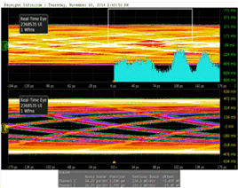
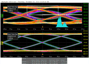
9.2.2 Sink Side Application
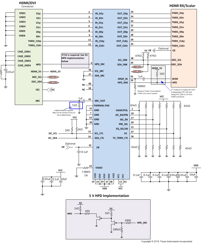
For a sink side application, HPD needs consideration. The TMDS181 drives the HPD signal to 3.3 V, which meets requirements, but if 5 V HPD signaling is required, the two circuits shown in Figure 35 are required. As sources are not consistent in implementing all aspects of the DDC link, TI recommends to configure the TMDS181 as per Figure 35. Another consideration for how HPD is implemented is the architecture and behavior of the HDMI RX/scalar. The standard requires sinks to clear the TMDS_CLOCK_RATIO_STATUS in the SCDC when either +5 V power signal from source is not present or when hot plug detect pin goes low for 100 ms or more. When HPD goes low, the TMDS181 automatically clears this bit. The TMDS181 expects the TMDS_CLOCK_RATIO_STATUS bit to be set with a write from source to receiver/sink. If this does not happen, the TMDS181 may come up in the wrong configuration. Until the HDMI ecosystem matures, TI recommends to implement sink application as per Figure 36 to address this.
Designing the TMDS181 into a sink side application requires similar care as for a source side application. However, because compliance is at the receiver, there is more flexibility for the transmitter to the HDMI RX/chipset link. Because many different reflection points are possible, the TMDS181 allows for swing, pre-emphasis, and transmitter termination control that can help minimize these reflections. The TMDS181 has a 3.3 V HPD drive capability which meets requirements. In cases where the designer needs to support 5 V HPD drive capability, the circuit shown in Figure 35 is required.
To design in the TMDS181 for a source side application, the designer must understand the following.
- Determine the loss profile between the RX/chipset and the HDMI/DVI connector
- Based upon this loss profile and signal swing, determine the optimal location for the TMDS181 to pass sink electrical compliance.
- Use the typical application Figure 35 for information on control pin resistors.
- The TMDS181 has a receiver adaptive equalizer, but can also be configured using EQ_SEL control pin.
- Set the VOD, pre-emphasis and termination levels appropriately to support a link between TMDS181 and HDMI RX/chipset by using the appropriate VSADJ resistor value and setting PRE_SEL and TX_TERM_CTL control pins.
- The thermal pad must be connected to ground.
- See schematics in Figure 35 on recommended decoupling capacitors from VCC pins to ground.
- Because the HDMI ecosystem supporting 4k2kp60 is not mature, TI recommends to design the TMDS181 into the sink application as shown in Figure 36.
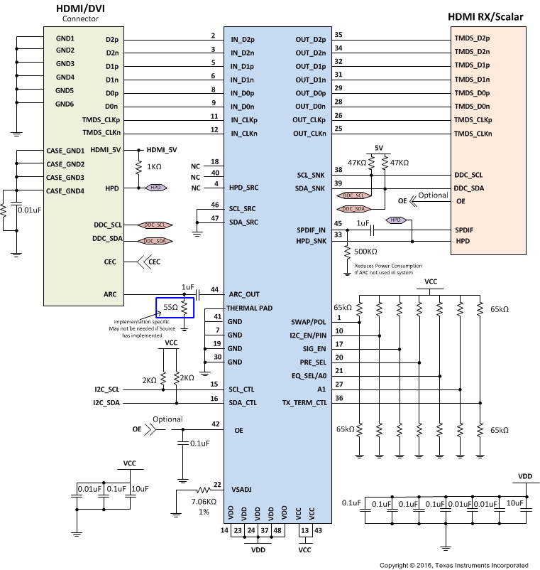 Figure 36. TMDS181 in Sink Side Application
9.2.3 Application Chain Showing DDC Connections
The DDC circuitry inside the TMDS181 allows multiple stage operation (see Figure 36). The retimer devices can be connected to any of the bus segments. The number of devices that can be connected in series is limited by repeater delay/time of flight considerations for the maximum bus speed requirements.
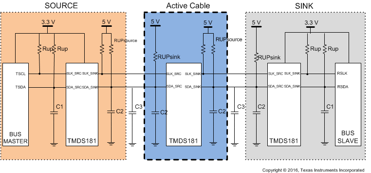 Figure 37. Typical Series Application
9.2.3.1 Detailed Design Procedure
9.2.3.1.1 DDC Pullup Resistors
NOTE
This section is informational only and subject to change depending upon the specific system implementation.
The pullup resistor value is determined by two requirements.
- The maximum sink current of the I2C buffer: The maximum sink current is 3 mA or slightly higher for an I2C driver supporting standard-mode I2C operation.
- The maximum transition time on the bus: The maximum transition time, T, of an I2C bus is set by an RC time constant. The parameter, k, can be calculated from Equation 3 by solving for t, the times at which certain voltage thresholds are reached. Different input threshold combinations introduce different values of t. Table 10 summarizes the possible values of k under different threshold combinations.
- R is the pullup resistor value.
- C is the total load capacitance.

where

Table 10. Value k upon Different Input Threshold Voltages
| Vth–\Vth+ | 0.7VCC | 0.65VCC | 0.6VCC | 0.55VCC | 0.5VCC | 0.45VCC | 0.4VCC | 0.35VCC | 0.3VCC |
|---|---|---|---|---|---|---|---|---|---|
| 0.1VCC | 1.0986 | 0.9445 | 0.8109 | 0.6931 | 0.5878 | 0.4925 | 0.4055 | 0.3254 | 0.2513 |
| 0.15VCC | 1.0415 | 0.8873 | 0.7538 | 0.6360 | 0.5306 | 0.4353 | 0.3483 | 0.2683 | 0.1942 |
| 0.2VCC | 0.9808 | 0.8267 | 0.6931 | 0.5754 | 0.4700 | 0.3747 | 0.2877 | 0.2076 | 0.1335 |
| 0.25VCC | 0.9163 | 0.7621 | 0.6286 | 0.5108 | 0.4055 | 0.3102 | 0.2231 | 0.1431 | 0.0690 |
| 0.3VCC | 0.8473 | 0.6931 | 0.5596 | 0.4418 | 0.3365 | 0.2412 | 0.1542 | 0.0741 |
From Equation 1, Rup(min) = 5.5 V / 3 mA = 1.83 kΩ to operate the bus under a 5 V pullup voltage and provide <3 mA when the I2C device is driving the bus to a low state. If a higher sink current, for example 4 mA, is allowed, Rup(min) can be as low as 1.375 kΩ. If DDC working at standard mode of 100 Kbps, the maximum transition time T is fixed, 1 μs, and using the k values from Table 10, the recommended maximum total resistance of the pullup resistors on an I2C bus can be calculated for different system setups. If DDC working in fast mode of 400 Kbps, the transition time should be set at 300 ns according to I2C specification. To support the maximum load capacitance specified in the HDMI specification, calculate Ccable(max) = 700 pF / Csource = 50 pF / Ci = 50 pF, R(max) as shown in Table 11.
Table 11. Pullup Resistor Upon Different Threshold Voltages and 800 pF Loads
| Vth-\Vth+ | 0.7VCC | 0.65VCC | 0.6VCC | 0.55VCC | 0.5VCC | 0.45VCC | 0.4VCC | 0.35VCC | 0.3VCC | UNIT |
|---|---|---|---|---|---|---|---|---|---|---|
| 0.1VCC | 1.14 | 1.32 | 1.54 | 1.8 | 2.13 | 2.54 | 3.08 | 3.84 | 4.97 | kΩ |
| 0.15VCC | 1.2 | 1.41 | 1.66 | 1.97 | 2.36 | 2.87 | 3.59 | 4.66 | 6.44 | kΩ |
| 0.2VCC | 1.27 | 1.51 | 1.8 | 2.17 | 2.66 | 3.34 | 4.35 | 6.02 | 9.36 | kΩ |
| 0.25VCC | 1.36 | 1.64 | 1.99 | 2.45 | 3.08 | 4.03 | 5.6 | 8.74 | 18.12 | kΩ |
| 0.3VCC | 1.48 | 1.8 | 2.23 | 2.83 | 3.72 | 5.18 | 8.11 | 16.87 | — | kΩ |
To accommodate the 3-mA drive current specification, a narrower threshold voltage range is required to support a maximum 800-pF load capacitance for a standard-mode I2C bus.
9.2.3.1.2 Compliance Testing
Compliance testing is very system design specific. Properly designing the system and configuring the TMDS181 can help pass compliance for a system. The following information is a starting point to help prepare for compliance testing. As each system is different there are many features in the TMDS181 to help tune the circuit. These include fixed RX equalization, adaptive RX equalization, VOD adjust by several methods, pre-emphasis/de-emphasis, and source termination. Passing both HDMI2.0a and HDMI1.4b compliance is easier to accomplish when using I2C as this provides more fine tuning capability.
9.2.3.1.2.1 Pin Strapping Configuration for HDMI2.0a and HDMI1.4b
9.2.3.1.2.2 I2C Control for HDMI2.0a and HDMI1.4b
- VSADJ Resistor = 7.06 kΩ: This value may be changed in order to improve Intra-pair skew but will increase VOD so care must be taken to avoid VOD and VL compliance issues. The VOD can be increased or decreased by using I2C Reg0Ch[7:2]
- PRE_SEL = Reg0Ch[1:0] = 01 for -2 dB (Labeled HDMI_TWPST)
- TX_TERM_CTL = NC for Auto Select.
- Reg0Bh[4:3] = 00 → No TX Term; HDMI1.4b < 2 Gbps (This may be best value for all HDMI1.4b)
- Reg0Bh[4:3] = 01 → 150 Ω to 300 Ω; HDMI1.4b > 2 Gbps
- Reg0Bh[4:3] = 11 → 75 Ω to 150 Ω; HDMI2.0a
