JAJSGR7C October   2014  – September 2018 TMP302-Q1

PRODUCTION DATA.  

  1. 特長
  2. アプリケーション
  3. 概要
    1.     Device Images
      1.      トリップ・スレッショルド精度
  4. 改訂履歴
  5. デバイス比較表
  6. Pin Configuration and Functions
    1.     Pin Functions
  7. Specifications
    1. 7.1 Absolute Maximum Ratings
    2. 7.2 ESD Ratings
    3. 7.3 Recommended Operating Conditions
    4. 7.4 Thermal Information
    5. 7.5 Electrical Characteristics
    6. 7.6 Typical Characteristics
  8. Detailed Description
    1. 8.1 Overview
    2. 8.2 Functional Block Diagram
    3. 8.3 Feature Description
      1. 8.3.1 HYSTSET
    4. 8.4 Device Functional Modes
  9. Application and Implementation
    1. 9.1 Application Information
      1. 9.1.1 Configuring the TMP302-Q1
    2. 9.2 Typical Application
      1. 9.2.1 Design Requirements
      2. 9.2.2 Detailed Design Procedure
      3. 9.2.3 Application Curves
  10. 10Power Supply Recommendations
  11. 11Layout
    1. 11.1 Layout Guidelines
    2. 11.2 Layout Example
  12. 12デバイスおよびドキュメントのサポート
    1. 12.1 ドキュメントの更新通知を受け取る方法
    2. 12.2 コミュニティ・リソース
    3. 12.3 商標
    4. 12.4 静電気放電に関する注意事項
    5. 12.5 Glossary
  13. 13メカニカル、パッケージ、および注文情報

パッケージ・オプション

メカニカル・データ(パッケージ|ピン)
サーマルパッド・メカニカル・データ
発注情報

Typical Characteristics

At TA = 25°C and VS = 3.3 V, unless otherwise noted.
TMP302-Q1 tc_trip_acc_err_temp_slos889.gif
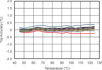
30 typical units
Figure 1. Trip Accuracy Error vs Temperature
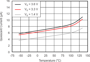
TMP302-Q1 tc_iq_temp_slos889.gif
Figure 2. Quiescent Current vs Temperature
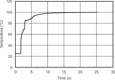
TMP302-Q1 tc_temp_step_resp_time_slos889.gif
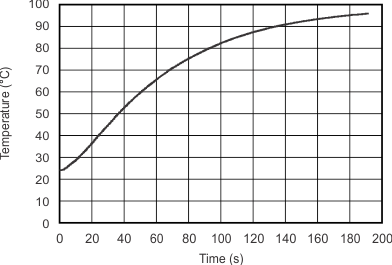
Figure 3. Temperature Step Response in Perfluorinated Fluid at 100°C vs Time
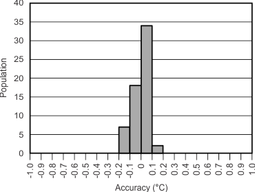
TMP302-Q1 tc_trip_thresh_histo_slos889.gif
Figure 5. Trip Threshold Accuracy
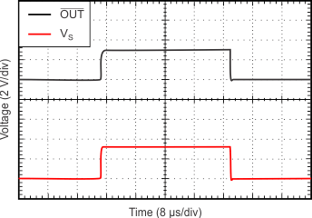
TMP302-Q1 tc_pu_pd_tr_slos889.gif
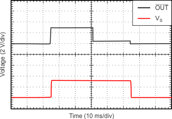
Figure 7. Power-Up and Power-Down Response
TMP302-Q1 tc_therm_step_resp_air_time_slos889.gif
Figure 4. Thermal Step Response in Air at 100°C vs Time
TMP302-Q1 tc_output_log_low_temp_slos889.gif
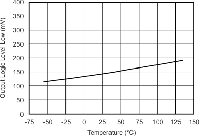
VS = 1.4 V IOL = 2 mA
Figure 6. Output Logic-Level Low VOL vs Temperature
TMP302-Q1 tc_pu_trip_pd_tr_slos889.gif
TMP302A-Q1, TA = 55°C TRIPSET1 = TRIPSET0 = GND
Figure 8. Power-Up, Trip, and Power-Down Response