JAJSI23I September 2009 – October 2019 TMP431 , TMP432
PRODUCTION DATA.
- 1 特長
- 2 アプリケーション
- 3 概要
- 4 改訂履歴
- 5 Pin Configuration and Functions
- 6 Specifications
- 7 Parameter Measurement Information
-
8 Detailed Description
- 8.1 Overview
- 8.2 Functional Block Diagram
- 8.3 Feature Description
- 8.4 Device Functional Modes
- 8.5 Programming
- 8.6
Register Maps
- 8.6.1 Pointer Register
- 8.6.2 Temperature Registers
- 8.6.3 Limit Registers
- 8.6.4 Status Registers
- 8.6.5 Configuration Register 1
- 8.6.6 Configuration Register 2
- 8.6.7 Conversion Rate Register
- 8.6.8 Beta Compensation Configuration Register
- 8.6.9 η-Factor Correction Register
- 8.6.10 Software Reset
- 8.6.11 Consecutive Alert Register
- 8.6.12 Therm Hysteresis Register
- 8.6.13 Identification Registers
- 8.6.14 Open Status Register
- 8.6.15 Channel Mask Register
- 8.6.16 High Limit Status Register
- 8.6.17 Low Limit Status Register
- 8.6.18 THERM Limit Status Register
- 9 Application and Implementation
- 10Power Supply Recommendations
- 11Layout
- 12デバイスおよびドキュメントのサポート
- 13メカニカル、パッケージ、および注文情報
6.7 Typical Characteristics
At TA = 25°C and V+ = 3.3 V, unless otherwise noted.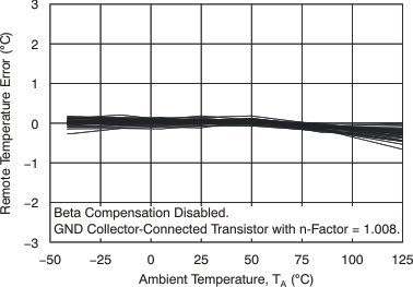 Figure 1. Remote Temperature Error vs Temperature
 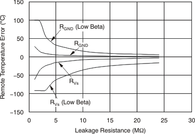 Figure 3. Remote Temperature Error vs Leakage Resistance
 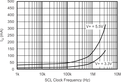 Figure 5. Shutdown Quiescent Current
vs SCL Clock Frequency
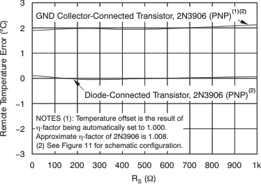 Figure 7. Remote Temperature Error vs Series Resistance
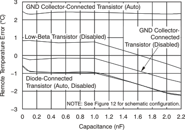
| At 25°C, V+ = 3.3 V, RS = 0 Ω |
vs Differential Capacitance
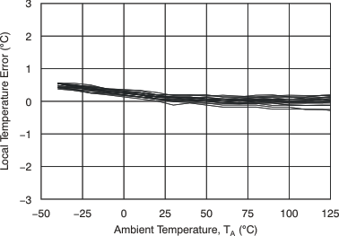 Figure 2. Local Temperature Error vs Temperature
 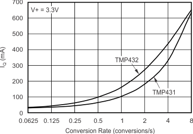 Figure 4. Quiescent Current vs Conversion Rate
 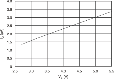 Figure 6. Shutdown Quiescent Current vs Supply Voltage
 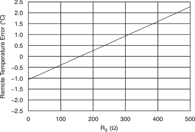 Figure 8. Remote Temperature Error vs Series Resistance
(Low-Beta Transistor)
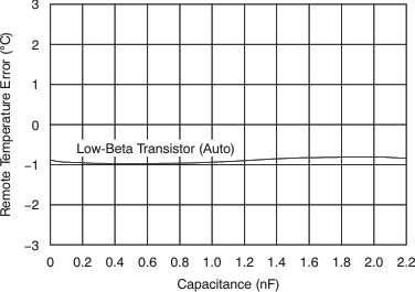
| At 25°C, V+ = 3.3 V, RS = 0 Ω, Beta = 011 (AUTO) |
vs Differential Capacitance With 45-nm CPU