JAJSGG9B November 2018 – February 2024 TMUX1108
PRODUCTION DATA
- 1
- 1 特長
- 2 アプリケーション
- 3 概要
- 4 Device Comparison Table
- 5 Pin Configuration and Functions
-
6 Specifications
- 6.1 Absolute Maximum Ratings
- 6.2 ESD Ratings
- 6.3 Recommended Operating Conditions
- 6.4 Thermal Information
- 6.5 Electrical Characteristics (VDD = 5V ±10 %)
- 6.6 Electrical Characteristics (VDD = 3.3V ±10 %)
- 6.7 Electrical Characteristics (VDD = 2.5V ±10 %), (VSS = –2.5V ±10 %)
- 6.8 Electrical Characteristics (VDD = 1.8V ±10 %)
- 6.9 Electrical Characteristics (VDD = 1.2V ±10 %)
- 6.10 Typical Characteristics
- 7 Detailed Description
- 8 Application and Implementation
- 9 Device and Documentation Support
- 10Revision History
- 11Mechanical, Packaging, and Orderable Information
パッケージ・オプション
メカニカル・データ(パッケージ|ピン)
サーマルパッド・メカニカル・データ
発注情報
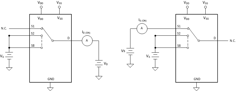
7.1.3 On-Leakage Current
Source on-leakage current is defined as the leakage current flowing into or out of the source pin when the switch is on. This current is denoted by the symbol IS(ON).
Drain on-leakage current is defined as the leakage current flowing into or out of the drain pin when the switch is on. This current is denoted by the symbol ID(ON).
Either the source pin or drain pin is left floating during the measurement. Figure 7-3 shows the circuit used for measuring the on-leakage current, denoted by IS(ON) or ID(ON).
 Figure 7-3 On-Leakage Measurement Setup